
Hot sale Factory 4 Layer Pcb Prototype - 14 Layer ENIG FR4 Buried Via PCB – Huihe
Hot sale Factory 4 Layer Pcb Prototype - 14 Layer ENIG FR4 Buried Via PCB – Huihe Detail:
About Blind Buried Via PCB
Blind vias and buried vias are two ways to establish connections between layers of printed circuit board. The blind vias of the printed circuit board are copper-plated vias that can be connected to the outer layer through most of the inner layer. The burrow connects two or more inner layers but does not penetrate the outer layer. Use microblind vias to increase line distribution density, improve radio frequency and electromagnetic interference, heat conduction, applied to servers, mobile phones, digital cameras.
Buried Vias PCB
The buried Vias connects two or more inner layers but does not penetrate the outer layer
|
Min Hole Diameter/mm |
Min ring/mm |
via-in-pad Diameter/mm |
Maximum Diameter/mm |
Aspect Ratio |
|
|
Blind Vias(conventional) |
0.1 |
0.1 |
0.3 |
0.4 |
1:10 |
|
Blind Vias(special product) |
0.075 |
0.075 |
0.225 |
0.4 |
1:12 |
Blind Vias PCB
Blind Vias is to connect an outer layer to at least one inner layer
|
|
Min. Hole Diameter/mm |
Minimum ring/mm |
via-in-pad Diameter/mm |
Maximum Diameter/mm |
Aspect Ratio |
|
Blind Vias(mechanical drilling) |
0.1 |
0.1 |
0.3 |
0.4 |
1:10 |
|
Blind Vias(Laser drilling) |
0.075 |
0.075 |
0.225 |
0.4 |
1:12 |
The advantage of blind Vias and buried Vias for engineers is the increase of component density without increasing layer number and size of circuit board. For electronic products with narrow space and small design tolerance, blind hole design is a good choice. The use of such holes helps the circuit design engineer to design a reasonable hole/pad ratio to avoid excessive ratios.
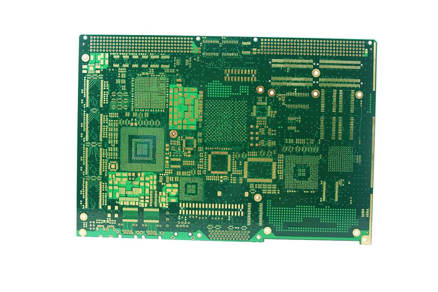
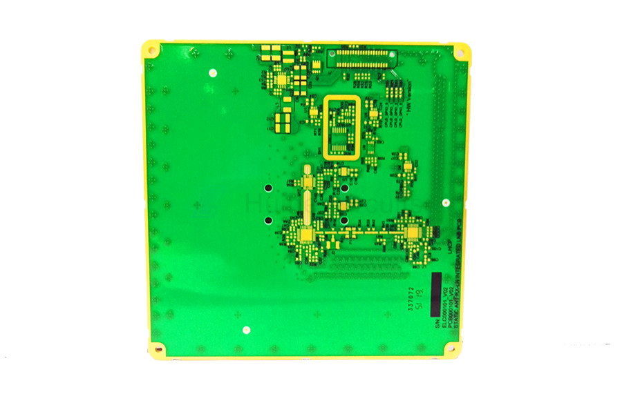
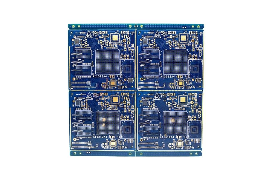
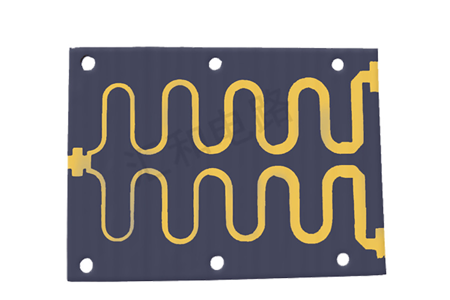
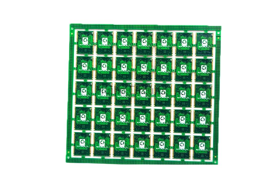
Product detail pictures:


Related Product Guide:
We love an incredibly fantastic standing amid our consumers for our superb item high quality, aggressive rate and also the finest assistance for Hot sale Factory 4 Layer Pcb Prototype - 14 Layer ENIG FR4 Buried Via PCB – Huihe , The product will supply to all over the world, such as: Albania, Sevilla, Orlando, The credibility is the priority, and the service is the vitality. We promise we have the ability to provide excellent quality and reasonable price products for customers. With us, your safety is guaranteed.
Sales manager is very enthusiastic and professional, gave us a great concessions and product quality is very good,thank you very much!
-
China Wholesale General Pcb Board Suppliers - ...
-
China Wholesale Electric Fence Circuit Board Su...
-
China Wholesale High Speed Pcb Factories - 2 L...
-

China Wholesale Motion Sensor Circuit Board Sup...
-

China Wholesale Pcb Board Supplier Quotes - 4 ...
-
China Wholesale Multisim Pcb Suppliers - 6 Lay...


