
Factory Price High Tg Pcb - 6 Layer HASL Blind Buried Via PCB – Huihe
Factory Price High Tg Pcb - 6 Layer HASL Blind Buried Via PCB – Huihe Detail:
Features Of The Buried Via PCB
The manufacturing process cannot be achieved by drilling after bonding. Drilling must be performed at individual circuit layers. The inner layer must be partially bonded first, followed by electroplating treatment, and then all bonded finally. This process is usually used only on high-density PCBs to increase the available space for other circuit layers
The Basic Process Of HDI Blind Buried Via PCB
Equipment Display

PCB Automatic Plating Line

PCB PTH Line

PCB LDI

PCB CCD Exposure Machine
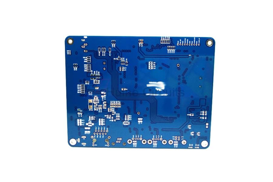
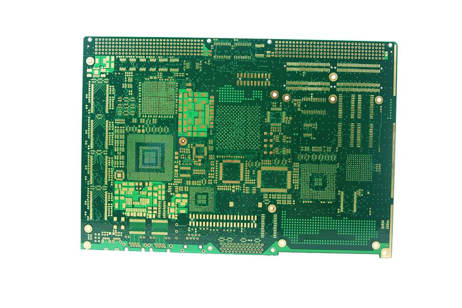
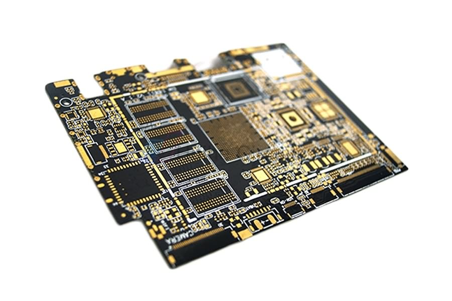
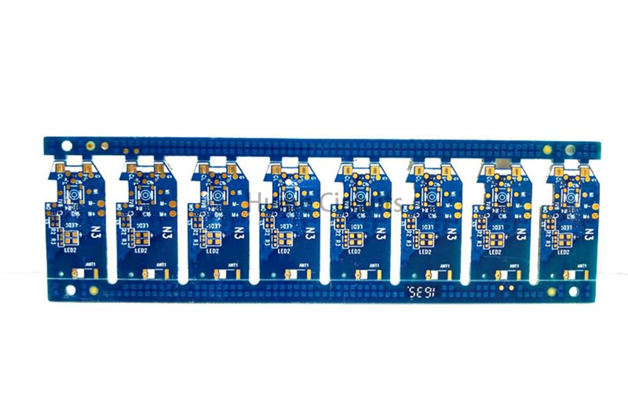
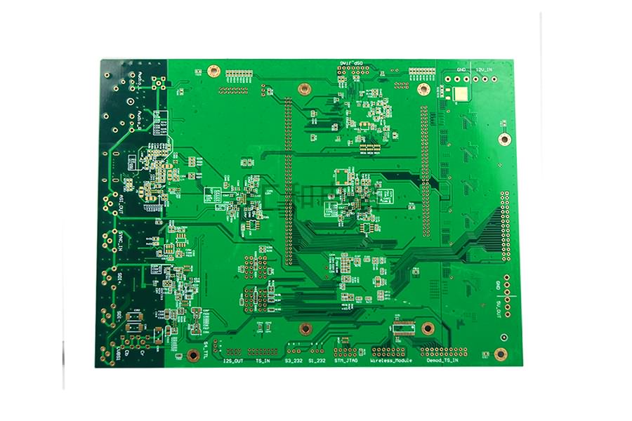
Product detail pictures:


Related Product Guide:
We goal to understand excellent disfigurement from the manufacturing and supply the top support to domestic and abroad clients wholeheartedly for Factory Price High Tg Pcb - 6 Layer HASL Blind Buried Via PCB – Huihe , The product will supply to all over the world, such as: Austria, Jeddah, Indonesia, Actually need to any of those objects be of interest to you, make sure you allow us to know. We'll be delighted to present you a quotation on receipt of one's comprehensive specs. We've our individual specialist R&D enginners to meet any of the requriements, We look forward to receiving your enquires soon and hope to have the chance to work together with you inside the future. Welcome to take a look at our organization.
It is really lucky to meet such a good supplier, this is our most satisfied cooperation, I think we will work again!
Write your message here and send it to us
-
China Wholesale Circuit Board Assembly Pricelis...
-
China Wholesale Ic Circuit Board Manufacturers ...
-
China Wholesale Rohs Circuit Board Quotes - 8 ...
-
China Wholesale Ic Pcb Board Manufacturers - 6...
-

China Wholesale Non Printed Circuit Board Suppl...
-

Online Exporter Bare Pcb Board - 6 Layer HASL ...


