
Competitive Price for Multi Layer Board - 14 Layer ENIG FR4 Buried Via PCB – Huihe
Competitive Price for Multi Layer Board - 14 Layer ENIG FR4 Buried Via PCB – Huihe Detail:
About Blind Buried Via PCB
Blind vias and buried vias are two ways to establish connections between layers of printed circuit board. The blind vias of the printed circuit board are copper-plated vias that can be connected to the outer layer through most of the inner layer. The burrow connects two or more inner layers but does not penetrate the outer layer. Use microblind vias to increase line distribution density, improve radio frequency and electromagnetic interference, heat conduction, applied to servers, mobile phones, digital cameras.
Buried Vias PCB
The buried Vias connects two or more inner layers but does not penetrate the outer layer
|
Min Hole Diameter/mm |
Min ring/mm |
via-in-pad Diameter/mm |
Maximum Diameter/mm |
Aspect Ratio |
|
|
Blind Vias(conventional) |
0.1 |
0.1 |
0.3 |
0.4 |
1:10 |
|
Blind Vias(special product) |
0.075 |
0.075 |
0.225 |
0.4 |
1:12 |
Blind Vias PCB
Blind Vias is to connect an outer layer to at least one inner layer
|
|
Min. Hole Diameter/mm |
Minimum ring/mm |
via-in-pad Diameter/mm |
Maximum Diameter/mm |
Aspect Ratio |
|
Blind Vias(mechanical drilling) |
0.1 |
0.1 |
0.3 |
0.4 |
1:10 |
|
Blind Vias(Laser drilling) |
0.075 |
0.075 |
0.225 |
0.4 |
1:12 |
The advantage of blind Vias and buried Vias for engineers is the increase of component density without increasing layer number and size of circuit board. For electronic products with narrow space and small design tolerance, blind hole design is a good choice. The use of such holes helps the circuit design engineer to design a reasonable hole/pad ratio to avoid excessive ratios.
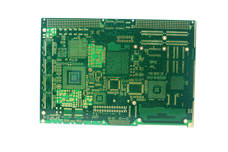
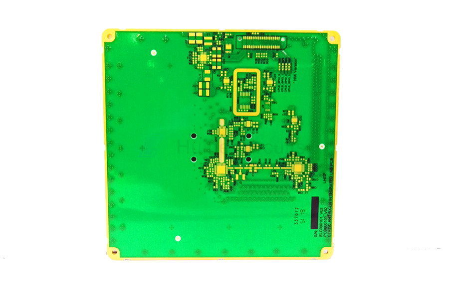
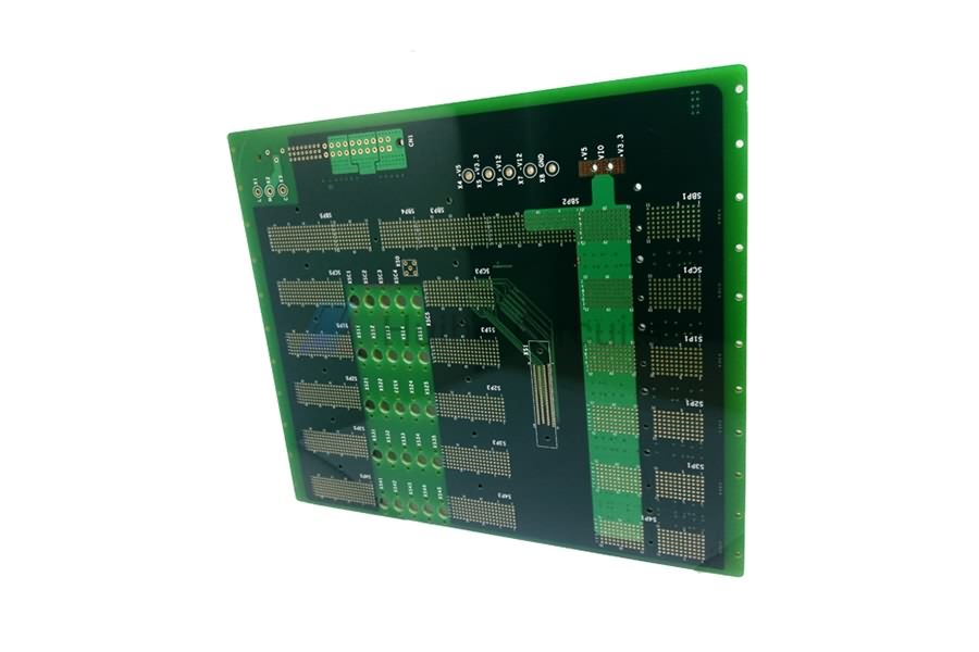
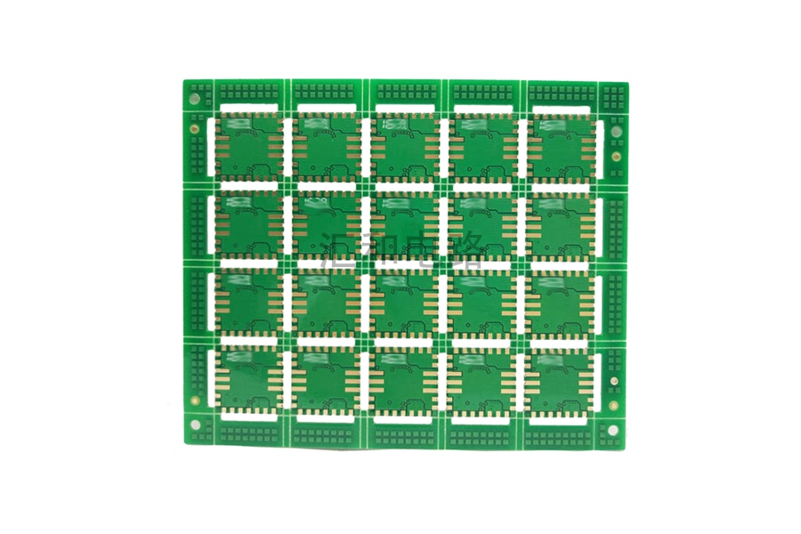
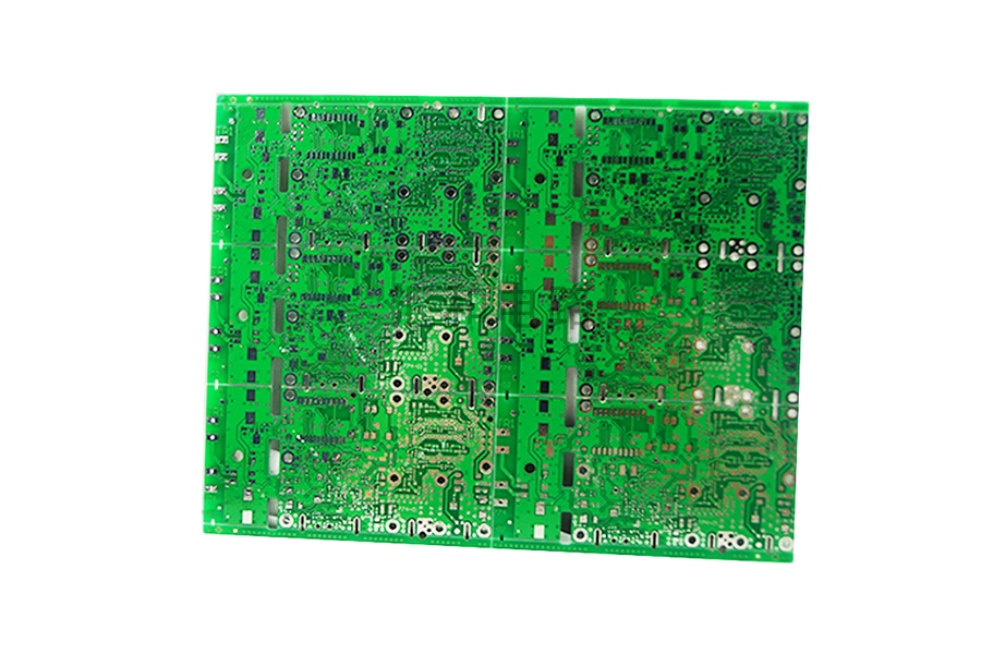
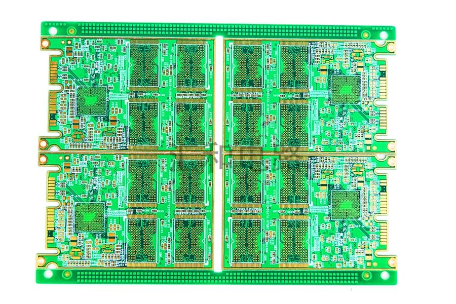
Product detail pictures:


Related Product Guide:
With our leading technology at the same time as our spirit of innovation,mutual cooperation, benefits and growth, we're going to build a prosperous future together with your esteemed firm for Competitive Price for Multi Layer Board - 14 Layer ENIG FR4 Buried Via PCB – Huihe , The product will supply to all over the world, such as: Colombia, Uruguay, azerbaijan, We are adhering to the philosophy of "attracting customers with the best products and excellent service". We welcome customers, business associations and friends from all parts of the world to contact us and seek cooperation for mutual benefits.
The factory workers have rich industry knowledge and operational experience, we learned a lot in working with them,we are extremely grateful that we can encount a good company has excellent wokers.
-
China Wholesale Ic Boards Quotes - 6 Layer FR4...
-
Short Lead Time for Prototype Pcb Board Manufac...
-

China Wholesale Solder Circuit Board Factories ...
-
China Wholesale Matte Black Pcb Suppliers - 4 ...
-
China Wholesale Red Pcb Manufacturers - 2 Laye...
-
China Wholesale Custom Printed Circuit Board Qu...


