
China Wholesale Wifi Pcb Board Suppliers - 4 Layer ENIG Blind Buried Via PCB – Huihe
China Wholesale Wifi Pcb Board Suppliers - 4 Layer ENIG Blind Buried Via PCB – Huihe Detail:
About The HDI PCB
Due to the influence of drilling tool, the cost of traditional PCB drilling is very high when the drilling diameter reaches 0.15mm, and it is difficult to improve again. The drilling of HDI PCB board no longer depends on the traditional mechanical drilling, but uses laser drilling technology. (so it is sometimes called laser plate.) The drilling hole diameter of HDI PCB board is generally 3-5mil (0.076-0.127mm), and the line width is generally 3-4mil (0.076-0.10mm). The size of pad can be greatly reduced, so more line distribution can be obtained in unit area, resulting in high-density interconnection.
The emergence of HDI technology adapts to and promotes the development of PCB industry. So that more dense BGA and QFP can be arranged in HDI PCB board. At present, HDI technology has been widely used, of which the first-order HDI has been widely used in the production of 0.5 pitch BGA PCB.
The development of HDI technology promotes the development of chip technology, which in turn promotes the improvement and progress of HDI technology.
At present, BGA chip of 0.5pitch has been widely used by design engineers, and the solder angle of BGA has gradually changed from the form of center hollowing out or center grounding to the form of center signal input and output needing wiring.
Advantages Of Blind Via And Buried Via PCB
The application of blind and buried via PCB can greatly reduce the size and quality of PCB, reduce the number of layers, improve the electromagnetic compatibility, increase the features of electronic products, reduce the cost, and make the design work more convenient and quick. In traditional PCB design and machining, through hole will bring many problems. First of all, they occupy a large amount of effective space. Secondly, a large number of through holes in one place also cause a huge obstacle to the routing of the inner layer of multi-layer PCB. These through holes occupy the space needed for routing. And conventional mechanical drilling will be 20 times as much work as non-perforating technology.
Factory Show

PCB Manufacturing Base

Admin Receptionist

Meeting Room

General Office
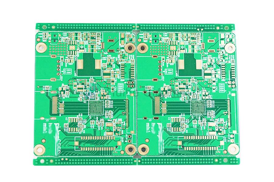
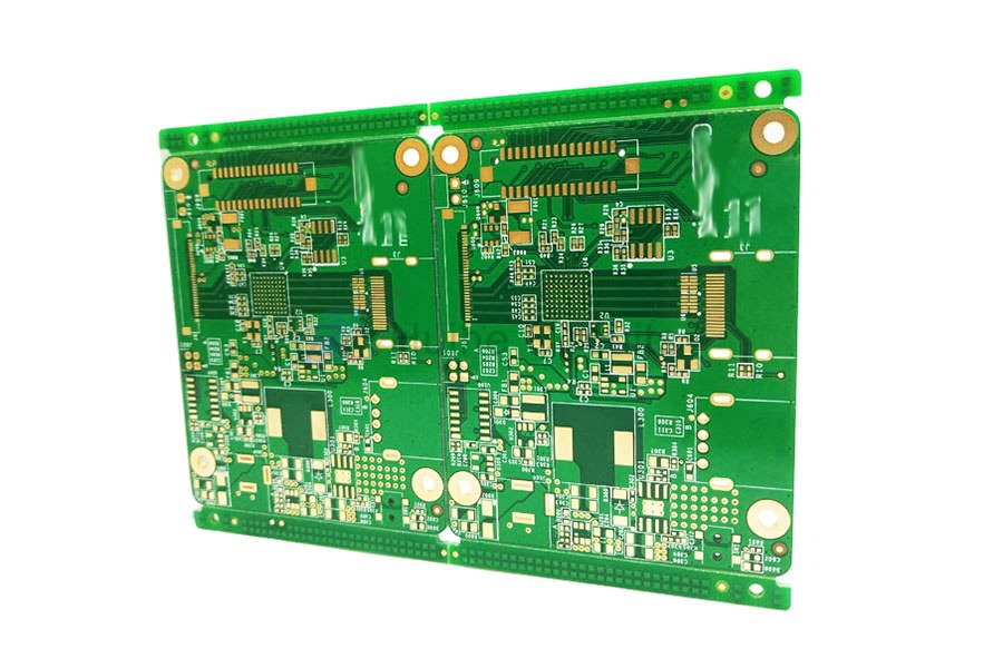
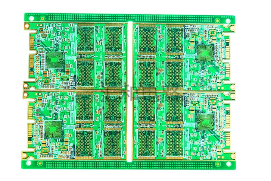
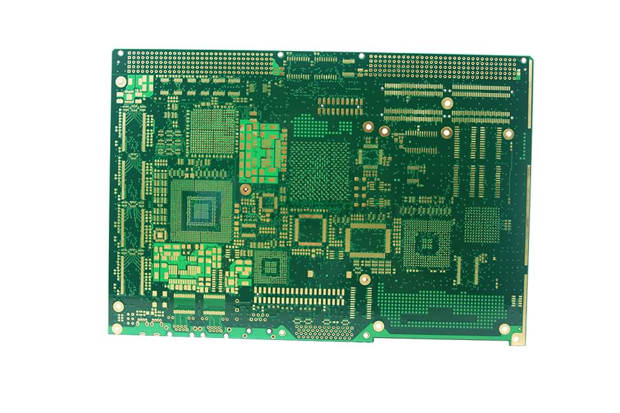
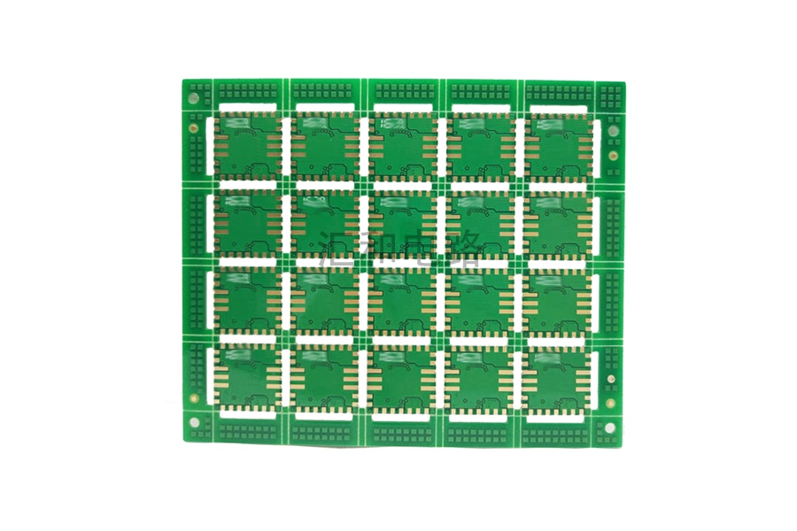
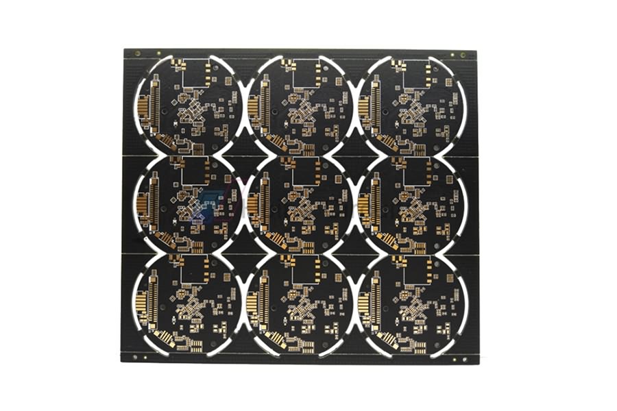
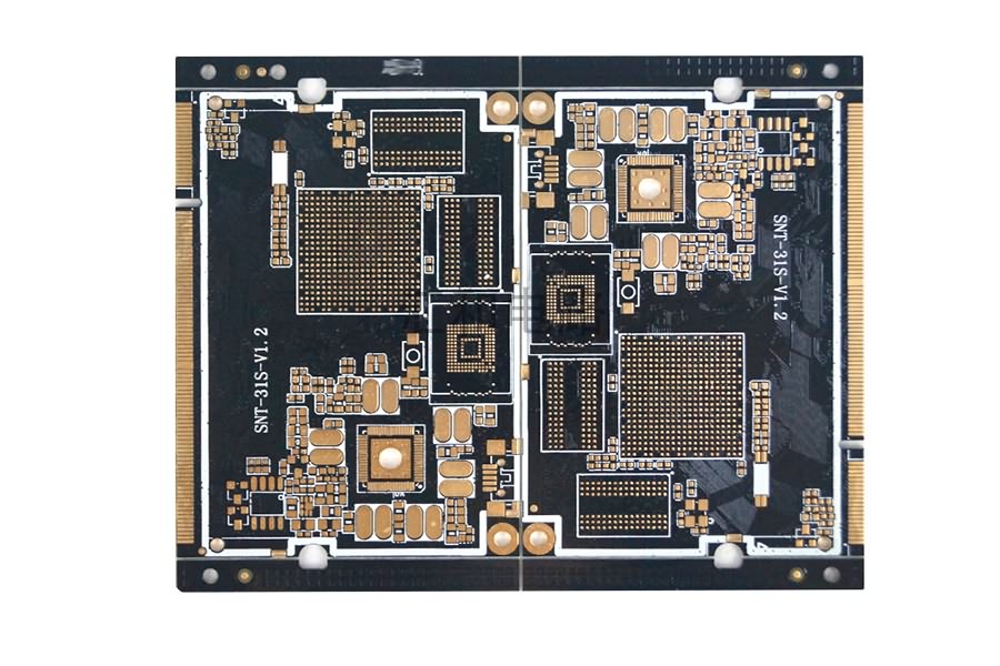
Product detail pictures:

Related Product Guide:
The key to our success is "Good Product Excellent, Reasonable Rate and Efficient Service" for China Wholesale Wifi Pcb Board Suppliers - 4 Layer ENIG Blind Buried Via PCB – Huihe , The product will supply to all over the world, such as: Amman, Mauritius, South Korea, It using the world's leading system for reliable operation, a low failure rate, it suitable for Argentina customers choice. Our company is situated within the national civilized cities, the traffic is very convenient, unique geographical and economic conditions. We pursue a people-oriented, meticulous manufacturing, brainstorm, build brilliant" business philosophy. Strict quality management, perfect service, reasonable price in Argentina is our stand on the premise of competition. If necessary, welcome to contact us by our website or phone consultation, we'll be happy to serve you.
We are really happy to find such a manufacturer that ensuring product quality at the same time the price is very cheap.
-
China Wholesale Silk Screen Printing Pcb Manufa...
-

China Wholesale Mini Pcb Board Suppliers - 2 l...
-
One of Hottest for Simple Pcb Board Supplier -...
-
China Wholesale Double Sided Pcb Board Prototyp...
-
China Wholesale Non Printed Circuit Board Price...
-
China Wholesale Flex Printed Circuit Board Pric...


