
China Wholesale Universal Pcb Quotes - 8 Layer ENIG Blind Buried Via PCB – Huihe
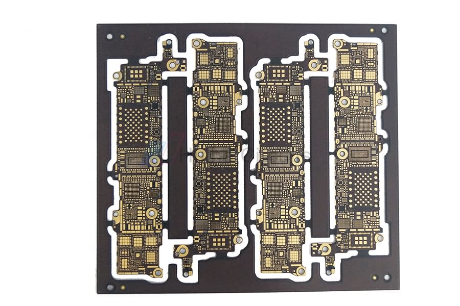
China Wholesale Universal Pcb Quotes - 8 Layer ENIG Blind Buried Via PCB – Huihe Detail:
About Level 1 HDI PCB
Level 1 HDI PCB technology refers to the laser blind hole only connected to the surface layer and its adjacent secondary layer hole forming technology.
pressing in one time after drilling →utside again pressing copper foil → and then laser drilling

About Level 1 HDI PCB
Level 2 HDI PCB
The Level 2 HDI PCB technology is an improvement on the Level 1 HDI PCB technology. It includes two forms of laser blind via drilling directly from the surface layer to the third layer, and laser blind hole drilling directly from the surface layer to the second layer and then from the second layer to the third layer. The difficulty of the Level 2 HDI PCB technology is far greater than the Level 1 HDI PCB technology.
Press in one time after drilling →outside again pressing copper foil →laser, drilling→outer again pressing copper foil→ laser drilling
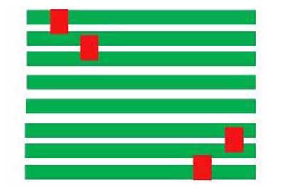
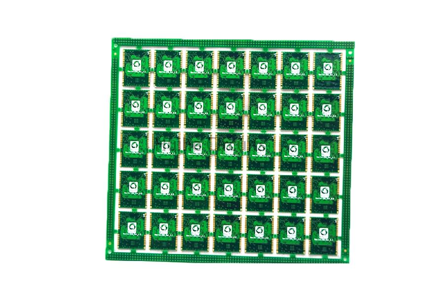
8 layers Of Double Via Level 1 HDI PCB
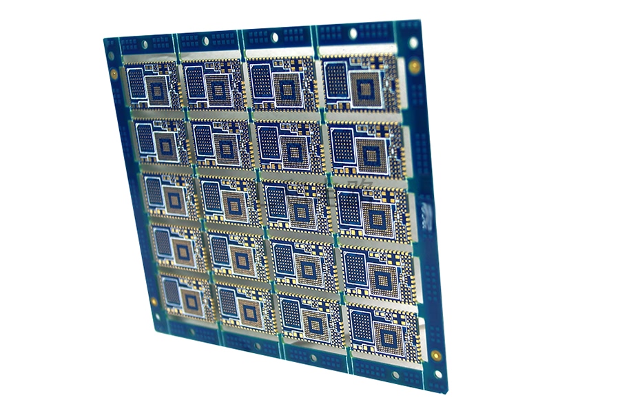
The figure below is 8 layers of level 2 cross blind vias , this processing methodand the above eight layers of second order stack hole , also need to play twolaser perforations . But the perforations are not stacked on top of each othermaking it much less difficult to process.
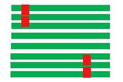
8 Layers Of Level 2 Cross Blind Vias PCB
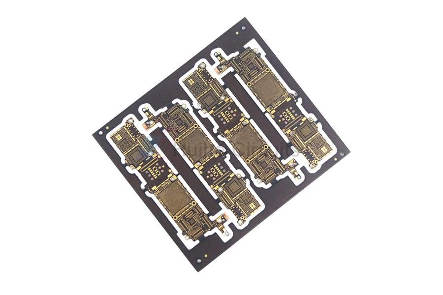
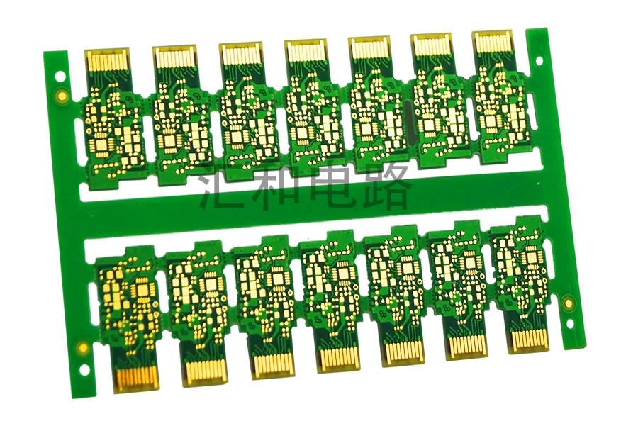
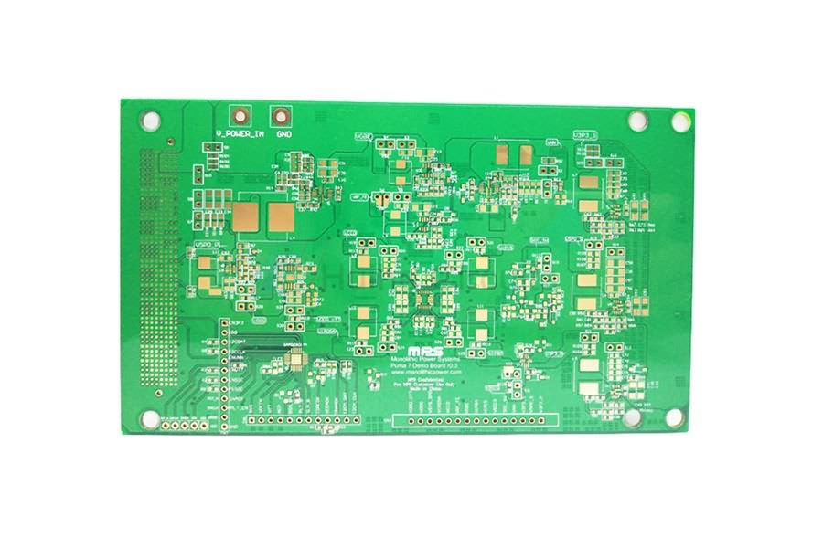
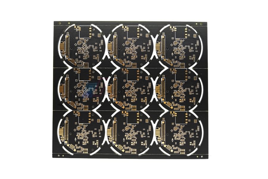
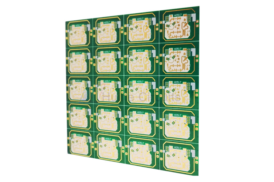
Product detail pictures:
Related Product Guide:
"Based on domestic market and expand overseas business" is our development strategy for China Wholesale Universal Pcb Quotes - 8 Layer ENIG Blind Buried Via PCB – Huihe , The product will supply to all over the world, such as: Bulgaria, Kazakhstan, South Korea, We have more than 200 staff including experienced managers, creative designers, sophisticated engineers and skilled workers. Through hard work of all employees for the past 20 years own company grew stronger and stronger. We always apply the "client first" principle. We also always fulfill all contracts to the point and therefore enjoy excellent reputation and trust among our customers. You are very welcome to personally visit our company.We hope to start a business partnership on the basis of mutual benefit and successful development . For more information please do no hesitate to contact us..
The product manager is a very hot and professional person, we have a pleasant conversation, and finally we reached a consensus agreement.
-
China Wholesale Stabilizer Circuit Board Manufa...
-
China Wholesale Emc Pcb Quotes - 4 Layer ENIG ...
-
China Wholesale Intercom Circuit Board Factorie...
-
China Wholesale Printed Circuit Board Manufactu...
-
China Wholesale Non Printed Circuit Board Price...
-
China Wholesale Redboard Pcb Factories - 4 Lay...


