
China Wholesale Teflon Pcb Board Factories - 6 Layer HASL Blind Buried Via PCB – Huihe
China Wholesale Teflon Pcb Board Factories - 6 Layer HASL Blind Buried Via PCB – Huihe Detail:
Features Of The Buried Via PCB
The manufacturing process cannot be achieved by drilling after bonding. Drilling must be performed at individual circuit layers. The inner layer must be partially bonded first, followed by electroplating treatment, and then all bonded finally. This process is usually used only on high-density PCBs to increase the available space for other circuit layers
The Basic Process Of HDI Blind Buried Via PCB
Equipment Display

PCB Automatic Plating Line

PCB PTH Line

PCB LDI

PCB CCD Exposure Machine
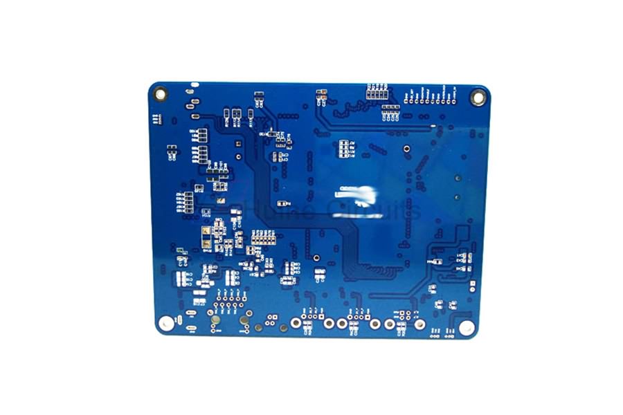
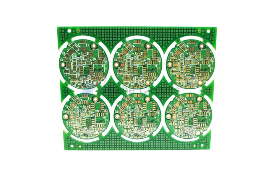
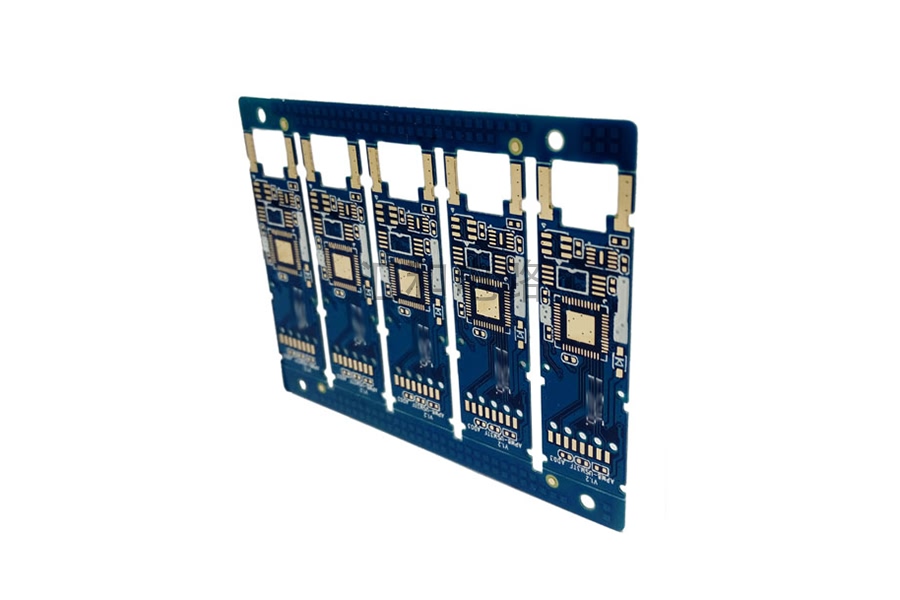
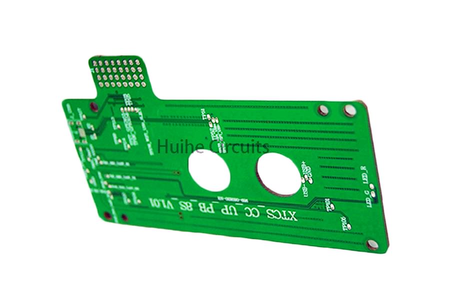
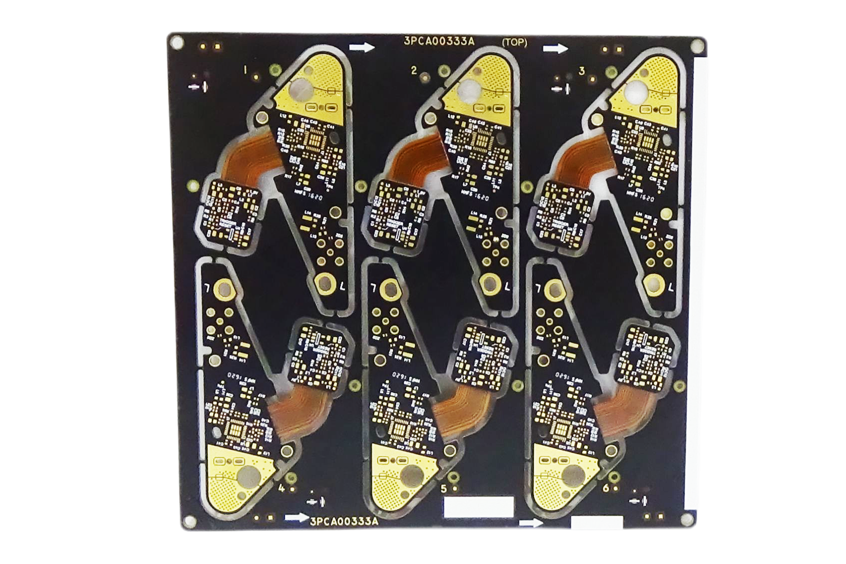
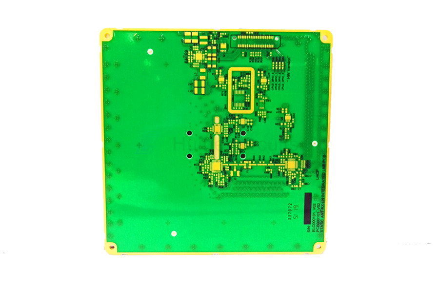
Product detail pictures:


Related Product Guide:
Our personnel are generally within the spirit of "continuous improvement and excellence", and using the excellent top quality goods, favorable rate and superior after-sales expert services, we try to win every customer's believe in for China Wholesale Teflon Pcb Board Factories - 6 Layer HASL Blind Buried Via PCB – Huihe , The product will supply to all over the world, such as: Melbourne, Angola, Hamburg, It is our customers' satisfaction over our products and services that always inspires us to do better in this business. We build mutually beneficial relationship with our clients by giving them large selection of premium car parts at marked down prices. We provide wholesale prices on all our quality parts so you are guaranteed greater savings.
We are a small company that has just started, but we get the company leader's attention and gave us a lot of help. Hope we can make progress together!
Write your message here and send it to us
-
High Quality Flexible Circuit Suppliers - 8 La...
-

China Wholesale Glc Pcb Pricelist - 4 Layer FR...
-
China Wholesale Printed Circuit Board Component...
-
China Wholesale Multilayer Flex Pcb Quotes - 1...
-
Cheap price Low Cost Pcb Manufacturing - 6 Lay...
-
China Wholesale Pcb Board Power Supply Pricelis...


