
China Wholesale Ssd Pcb Pricelist - 6 Layer HASL Blind Buried Via PCB 13699 – Huihe
China Wholesale Ssd Pcb Pricelist - 6 Layer HASL Blind Buried Via PCB 13699 – Huihe Detail:
Features of the Buried Via
The manufacturing process cannot be achieved by drilling after bonding. Drilling must be performed at individual circuit layers. The inner layer must be partially bonded first, followed by electroplating treatment, and then all bonded finally. This process is usually used only on high-density PCBs to increase the available space for other circuit layers
The basic process of making HDI blind buried Via PCB
Equipment display

Automatic Plating Line

PTH line

LDI

CCD Exposure Machine
Application

Communications

Security electronics

Railtransit
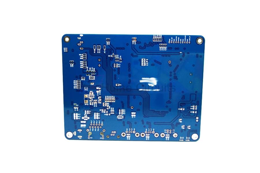
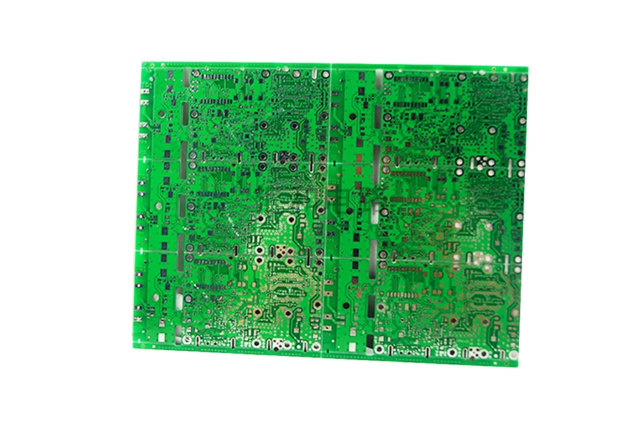
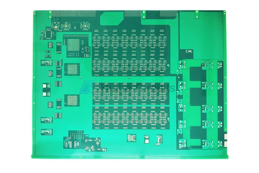
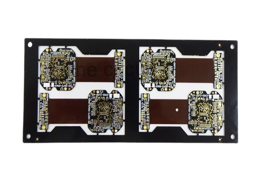
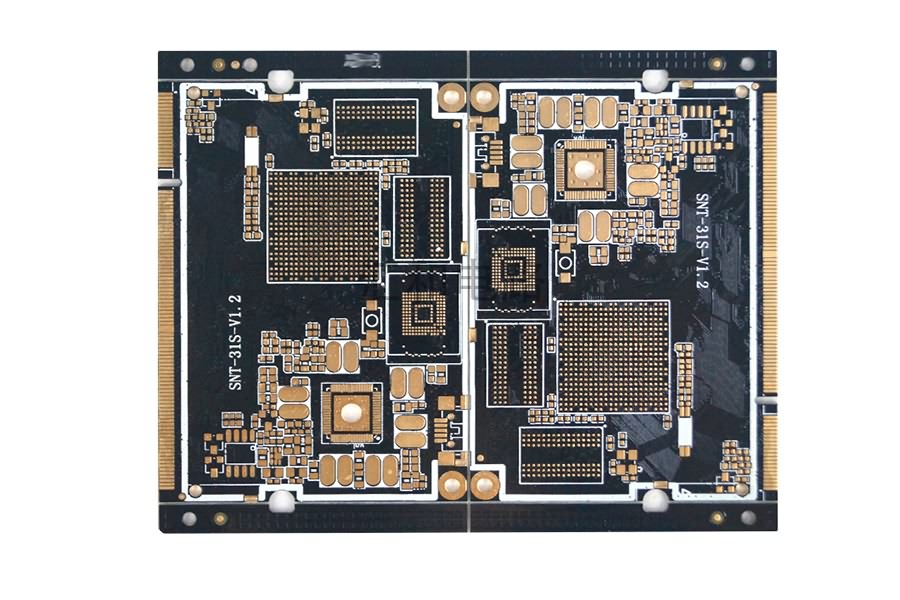
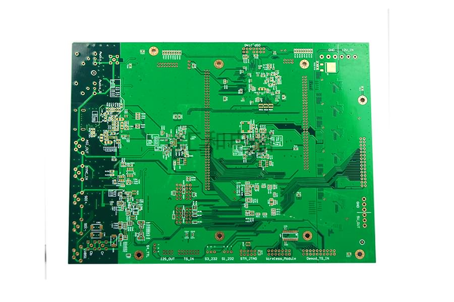
Product detail pictures:


Related Product Guide:
With our leading technology also as our spirit of innovation,mutual cooperation, benefits and development, we are going to build a prosperous future jointly with your esteemed company for China Wholesale Ssd Pcb Pricelist - 6 Layer HASL Blind Buried Via PCB 13699 – Huihe , The product will supply to all over the world, such as: Zambia, Malaysia, Iran, We've a skilled sales team, they have mastered the best technology and manufacturing processes, have years of experience in foreign trade sales, with customers able to communicate seamlessly and accurately understand the real needs of customers, providing customers with personalized service and unique merchandise.
Staff is skilled, well-equipped, process is specification, products meet the requirements and delivery is guaranteed, a best partner!
Write your message here and send it to us
-
China Wholesale Electric Fence Circuit Board Pr...
-
China Wholesale Panel Circuit Board Pricelist -...
-
China Wholesale Stabilizer Pcb Board Quotes - ...
-
China Wholesale Hal Pcb Pricelist - 6 Layer EN...
-
China Wholesale Mini Pcb Board Quotes - 6 Laye...
-
China Wholesale Fast Turn Pcb Factories - 6 La...


