
China Wholesale Small Pcb Board Factories - 14 Layer Blind Buried Via PCB – Huihe
China Wholesale Small Pcb Board Factories - 14 Layer Blind Buried Via PCB – Huihe Detail:
About Blind Buried Via PCB
Blind vias and buried vias are two ways to establish connections between layers of printed circuit board. The blind vias of the printed circuit board are copper-plated vias that can be connected to the outer layer through most of the inner layer. The burrow connects two or more inner layers but does not penetrate the outer layer. Use microblind vias to increase line distribution density, improve radio frequency and electromagnetic interference, heat conduction, applied to servers, mobile phones, digital cameras.
Buried Vias PCB
The buried Vias connects two or more inner layers but does not penetrate the outer layer
|
Min Hole Diameter/mm |
Min ring/mm |
via-in-pad Diameter/mm |
Maximum Diameter/mm |
Aspect Ratio |
|
|
Blind Vias(conventional) |
0.1 |
0.1 |
0.3 |
0.4 |
1:10 |
|
Blind Vias(special product) |
0.075 |
0.075 |
0.225 |
0.4 |
1:12 |
Blind Vias PCB
Blind Vias is to connect an outer layer to at least one inner layer
|
|
Min. Hole Diameter/mm |
Minimum ring/mm |
via-in-pad Diameter/mm |
Maximum Diameter/mm |
Aspect Ratio |
|
Blind Vias(mechanical drilling) |
0.1 |
0.1 |
0.3 |
0.4 |
1:10 |
|
Blind Vias(Laser drilling) |
0.075 |
0.075 |
0.225 |
0.4 |
1:12 |
The advantage of blind Vias and buried Vias for engineers is the increase of component density without increasing layer number and size of circuit board. For electronic products with narrow space and small design tolerance, blind hole design is a good choice. The use of such holes helps the circuit design engineer to design a reasonable hole/pad ratio to avoid excessive ratios.
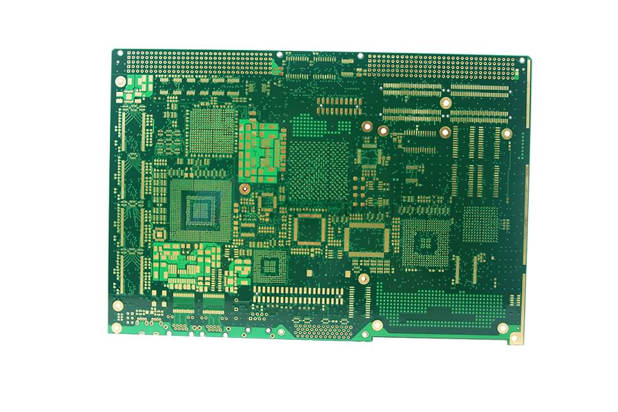
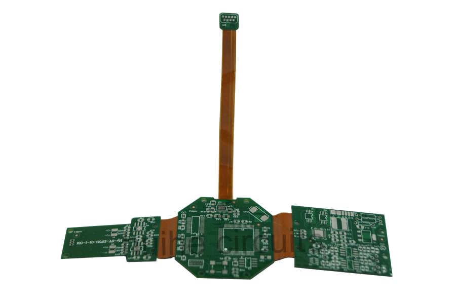
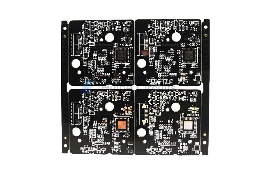
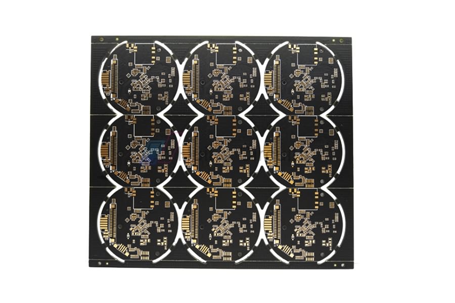
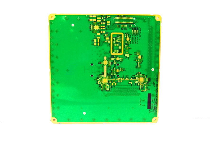
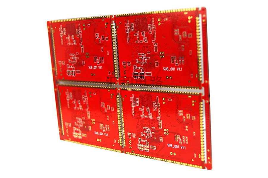
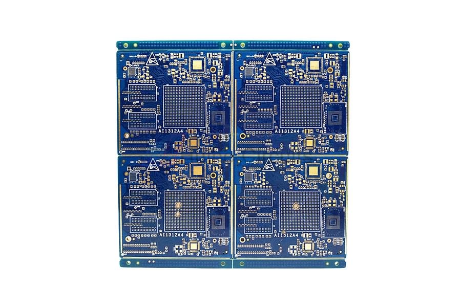
Product detail pictures:


Related Product Guide:
We always do the job to be a tangible group making sure that we can provide you with the top top quality as well as ideal value for China Wholesale Small Pcb Board Factories - 14 Layer Blind Buried Via PCB – Huihe , The product will supply to all over the world, such as: Cape Town, Johannesburg, Oman, Our items are widely recognized and trusted by users and can meet continuously changing economic and social needs. We welcome new and old customers from all walks of life to contact us for future business relationships and mutual success!
This is the first business after our company establish, products and services are very satisfying, we have a good start, we hope to cooperate continuous in the future!
-
China Wholesale Circuit Board Assembly Factorie...
-
China Wholesale Pcb Board Components Quotes - ...
-
China Wholesale Flexible Pcb Fabrication Factor...
-
China Wholesale Quick Turn Flex Circuits Pricel...
-
China Wholesale Polyimide Flex Pcb Factories -...
-
China Wholesale Impedance Control In Pcb Pricel...


