
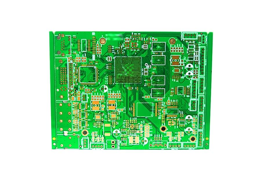
China Wholesale Silk Screen Printing Pcb Manufacturers - 6 Layer HASL Blind Buried Via PCB – Huihe
China Wholesale Silk Screen Printing Pcb Manufacturers - 6 Layer HASL Blind Buried Via PCB – Huihe Detail:
Features Of The Buried Via PCB
The manufacturing process cannot be achieved by drilling after bonding. Drilling must be performed at individual circuit layers. The inner layer must be partially bonded first, followed by electroplating treatment, and then all bonded finally. This process is usually used only on high-density PCBs to increase the available space for other circuit layers
The Basic Process Of HDI Blind Buried Via PCB
Equipment Display

PCB Automatic Plating Line

PCB PTH Line

PCB LDI

PCB CCD Exposure Machine
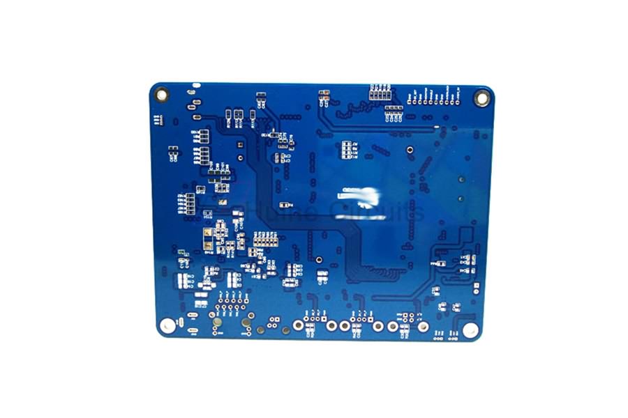
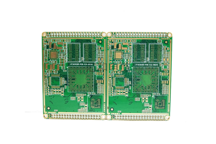
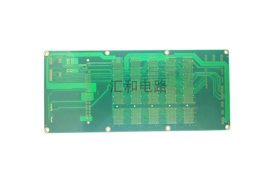
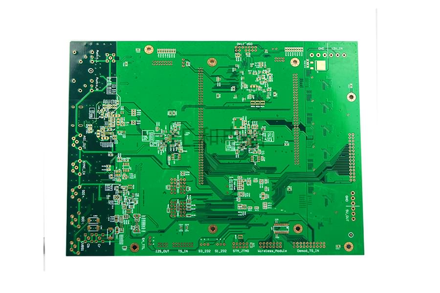
Product detail pictures:


Related Product Guide:
We can easily normally satisfy our respected buyers with our excellent high-quality, excellent selling price and good service due to we've been far more expert and more hard-working and do it in cost-effective way for China Wholesale Silk Screen Printing Pcb Manufacturers - 6 Layer HASL Blind Buried Via PCB – Huihe , The product will supply to all over the world, such as: New Orleans, Toronto, Turkey, Thus far, our item associated with printer dtg a4 may be shown in most foreign nations as well as urban centers, which are sought after simply by targeted traffic. We all highly imagine that now we have the full capacity to present you with contented merchandise. Desire to collect requests of your stuff and produce the long-term co-operation partnership. We very seriously promise:Csame top quality, better price; exact same selling price, higher quality.
High production efficiency and good product quality, fast delivery and completed after-sale protection, a right choice, a best choice.
Write your message here and send it to us
-
China Wholesale Ptfe Pcb Pricelist - 6 Layer E...
-
China Wholesale Round Pcb Quotes - 6 Layer ENI...
-
China Wholesale Glc Pcb Factories - 6 Layer EN...
-
China Wholesale Surface Mount Prototype Board P...
-
China Wholesale Small Pcb Board Quotes - 6 lay...
-

China Wholesale Pcba Circuit Board Quotes - 6 ...


