
China Wholesale Prototype Pcb Quotes - 6 Layer ENIG Impedance Control PCB – Huihe
China Wholesale Prototype Pcb Quotes - 6 Layer ENIG Impedance Control PCB – Huihe Detail:
Difference Between Pad And Via
1. Definitions Differ
Pad: is the basic unit of surface mount assembly, which is used to form the landpattern of the circuit board, that is, a variety of combinations of pads designed for special component types.
Through hole: through hole is also called metallization hole. In the double panel and multilayer PCB, a common hole is drilled at the junction of the wires that need to be connected between the layers in order to connect the printed wires between layers. The main parameters of the hole are the outer diameter of the hole and the size of the hole.
The hole itself has parasitic capacitance and inductance to the ground, which often brings great negative effect to the circuit design.
2. Different Principles
Pad: When a pad structure is not designed correctly, it is difficult to reach the desired weld point. Can be used for surface-mounted components or for plug-in components.
Through hole: In a circuit board, a line jumps from one side of the board to the other. The hole connecting the two wires is also called a hole (as opposed to a pad, there is no solder layer on the side). Also known as metallization hole, in the double panel and multilayer PCB, for connecting the printed wire between the layers, in each layer need to be connected at the intersection of the wire drilling on a public hole, that is, through the hole.
Technically, a layer of metal is PCB on the cylindrical surface of the hole wall of the hole through the chemical deposition method to connect the copper foil that needs to be connected in the middle layer, and the upper and lower sides of the hole through the shape of a circular solder pad, the parameters of the hole mainly include the outer diameter of the hole and the size of the hole.
3. Different Effects
Through hole: the hole on PCB, play the role of conduction or heat dissipation.
Pad: it is the copper plate of PCB, some cooperate with the hole to connect, and some square plate, mainly used to paste parts.
Equipment Display

PCB Automatic Plating Line

PCB PTH Line

PCB LDI

PCB CCD Exposure Machine
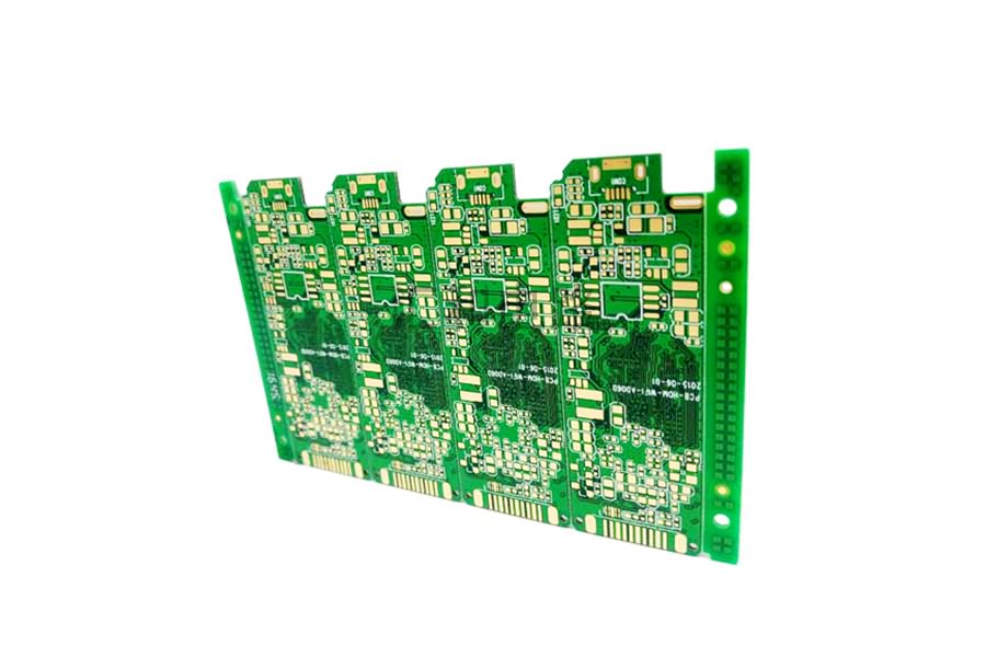
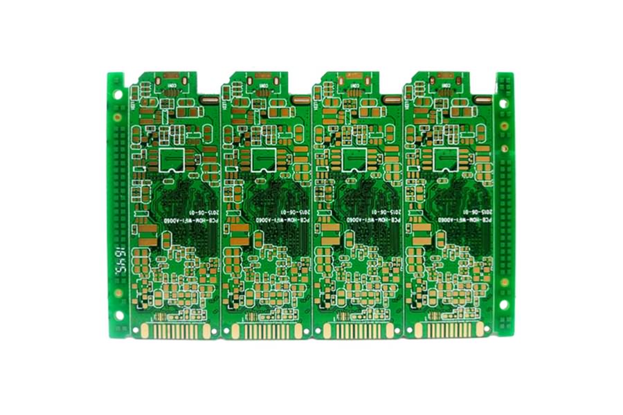
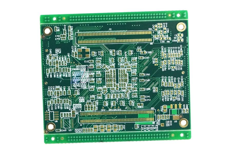
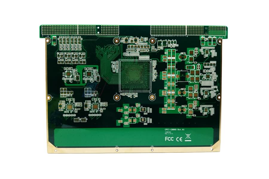
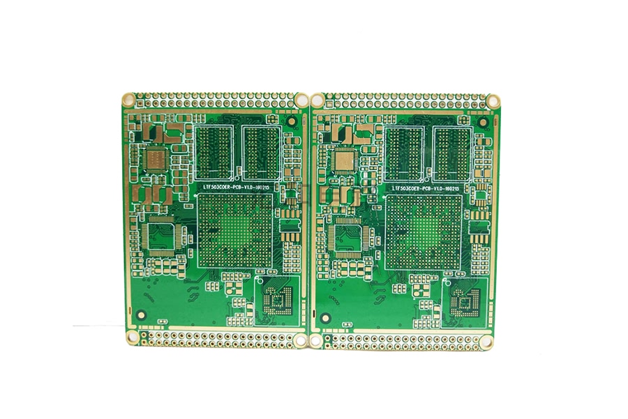
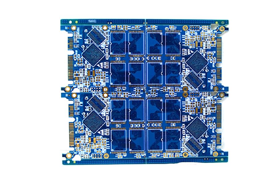
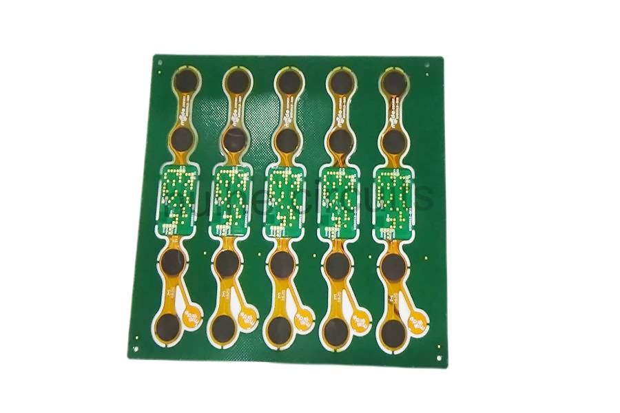
Product detail pictures:


Related Product Guide:
Assume full accountability to satisfy all demands of our consumers; reach ongoing advancements by endorsing the expansion of our purchasers; come to be the final permanent cooperative partner of clients and maximize the interests of clientele for China Wholesale Prototype Pcb Quotes - 6 Layer ENIG Impedance Control PCB – Huihe , The product will supply to all over the world, such as: Puerto Rico, Belize, United Arab Emirates, Our solutions have national accreditation standards for experienced, premium quality items, affordable value, was welcomed by people around the globe. Our goods will continue to increase in the order and look forward to cooperation with you, Really should any of those products be of interest to you, please letus know. We are going to be pleased to give you a quotation up on receipt of one's detailed specifications.
In China, we have purchased many times, this time is the most successful and most satisfactory, a sincere and realiable Chinese manufacturer!
-
China Wholesale Main Pcb Board Manufacturers -...
-
China Wholesale Custom Circuit Board Factories ...
-
Super Lowest Price 4 Layer Fpc Supplier - 6 La...
-
PriceList for Automatic Stabilizer Circuit Boar...
-
China Wholesale High Quality Pcb Quotes - 4 La...
-
China Wholesale Production Of Pcb Pricelist - ...


