
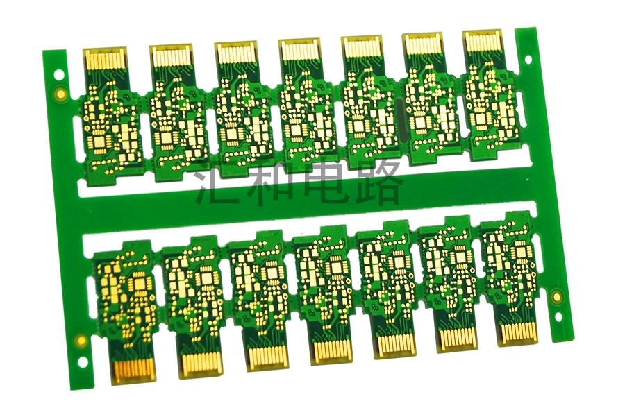
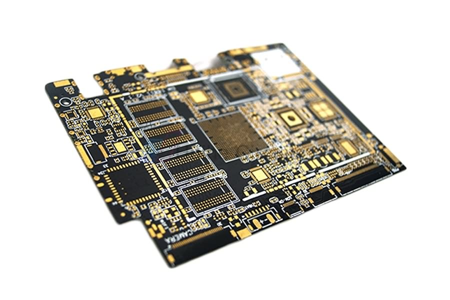
China Wholesale Prototype Pcb Manufacturers - 10 Layer ENIG Blind Vias PCB – Huihe
China Wholesale Prototype Pcb Manufacturers - 10 Layer ENIG Blind Vias PCB – Huihe Detail:
About Blind Buried Via PCB
Blind Via: which enables the connection and conduction between the inner and outer layers
Buried Via: which can connect and guide between inner layers Blind Vias are mostly small holes with a diameter of 0.05mm~0.15mm. There are laser hole forming, plasma etched hole and photoinduced hole forming, and laser hole forming is usually used.
HDI: High-density interconnection, non-mechanical drilling, micro-blind hole ring below 6mil, inside and outside layers of wiring line width/line gap is below 4mil, the diameter of the pad is not greater than 0.35mm is called HDI board production mode.
Blind Vias
Blind Vias are used to connect one outer layer to at least one inner layer. Each layer of blind hole needs to generate a separate drill file. The ratio of hole depth to aperture (aspect ratio/thickness-diameter ratio) must be less than or equal to 1. The keyhole determines the hole depth, that is, the maximum distance between the outermost layer and the inner layer.
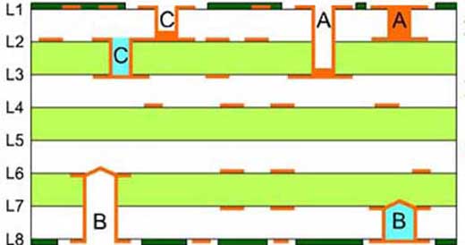
A: Laser drilling of blind vias
B: Mechanical drilling of blind vias
C: Cross blind via
Equipment Display

PCB Automatic Plating Line

PCB PTH Line

PCB LDI

PCB CCD Exposure Machine
Factory Show

PCB Manufacturing Base

Admin Receptionist

Meeting Room

General Office
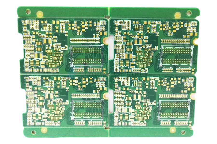
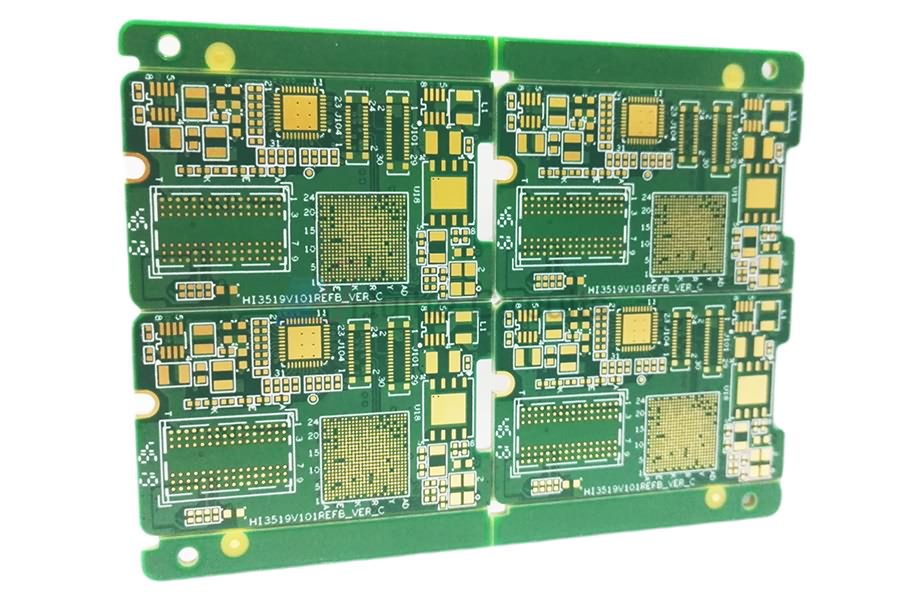
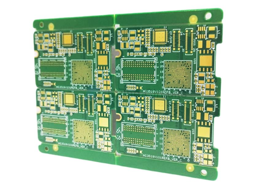
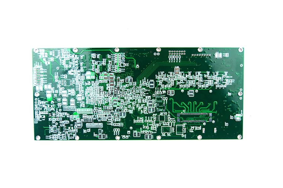
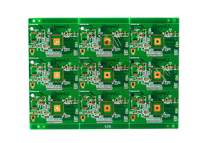
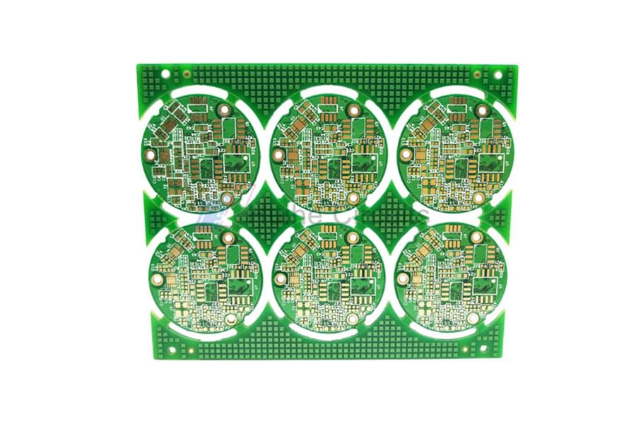
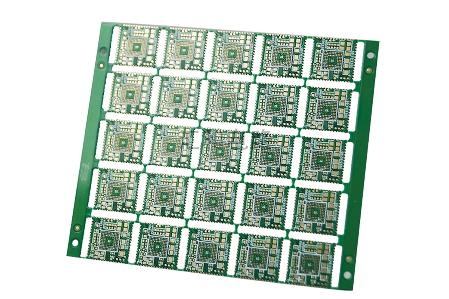
Product detail pictures:

Related Product Guide:
Using a full scientific good quality administration system, very good quality and superior faith, we win good standing and occupied this discipline for China Wholesale Prototype Pcb Manufacturers - 10 Layer ENIG Blind Vias PCB – Huihe , The product will supply to all over the world, such as: Mumbai, Nepal, Japan, Our products are widely sold to Europe, USA, Russia, UK, France, Australia, Middle East, South America, Africa, and Southeast Asia, etc. Our products are highly recognized by our customers from all around the world. And our company is committed to continually improving effectiveness of our management system to maximize customer satisfaction. We sincerely hope to make progress with our customers and create a win-win future together. Welcome to join us for business!
This is a very professional and honest Chinese supplier, from now on we fell in love with the Chinese manufacturing.
-
China Wholesale Prototype Pcb Assembly Quotes -...
-
Hot New Products Rigid Flex Circuit Board - 4 ...
-
China Wholesale Pcb Speaker Pricelist - 8 Laye...
-
China Wholesale Pcb Order Pricelist - 4 Layer ...
-
China Wholesale Round Pcb Suppliers - 6 Layer...
-
China Wholesale Printed Wiring Board Assembly S...


