
China Wholesale Pcb Via In Pad Factories - 2 Layer ENIG Heavy Copper PCB – Huihe
China Wholesale Pcb Via In Pad Factories - 2 Layer ENIG Heavy Copper PCB – Huihe Detail:
Difficulties In Drilling Heavy Copper PCBs
With the increase of the copper thickness, the thickness of the heavy copper PCB also increases. heavy copper PCB is usually more than 2.0mm thick, drilling production due to the thickness of the thickness of the plate and copper thick factors, production is more difficult. In this regard, the use of a new cutter, reduce the service life of the drill cutter, section drilling has become an effective solution to the heavy copper PCB drilling. In addition, the optimization of drilling parameters such as feed speed and rewind speed also has a great influence on the quality of the hole.
The problem of milling target holes. During drilling, the energy of X-Ray gradually decreases with the increase of copper thickness, and its penetration capacity reaches the upper limit. Therefore, for PCB with thick copper thickness, it is impossible to confirm the deviation of the head plate during drilling. In this regard, the offset confirmation target can be set at different positions of the plate edge, and the offset confirmation target is first milled out in accordance with the target position in the data on the copper foil at the time of cutting, and the target hole on the copper foil and the inner layer target hole are produced in accordance with the lamination.
Equipment Display

PCB Automatic Plating Line

PCB PTH Line

PCB LDI

PCB CCD Exposure Machine
Factory Show

PCB Manufacturing Base

Admin Receptionist

Meeting Room

General Office
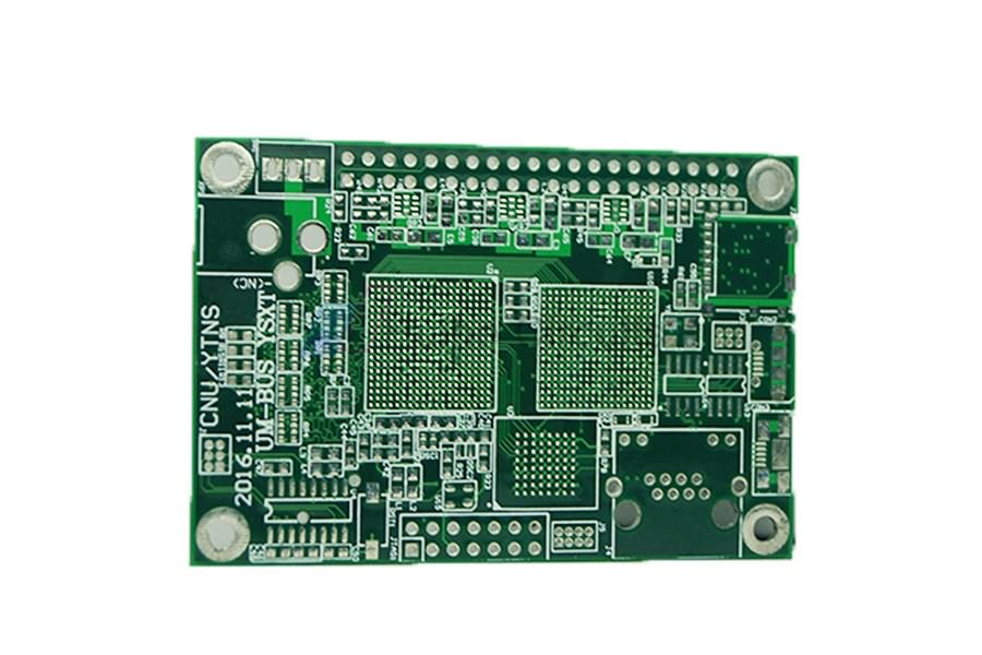
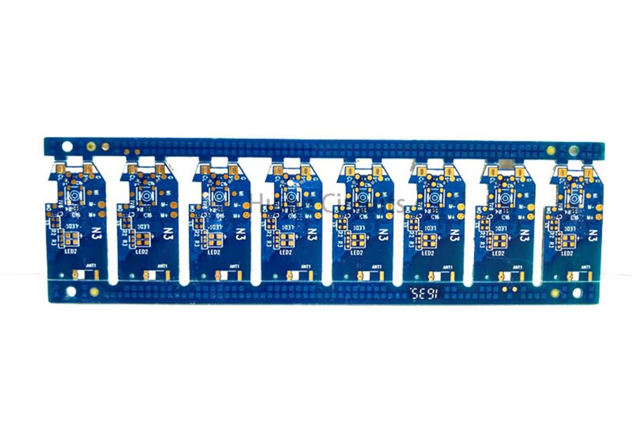
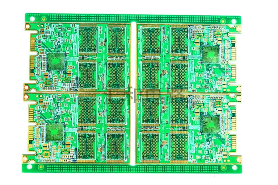
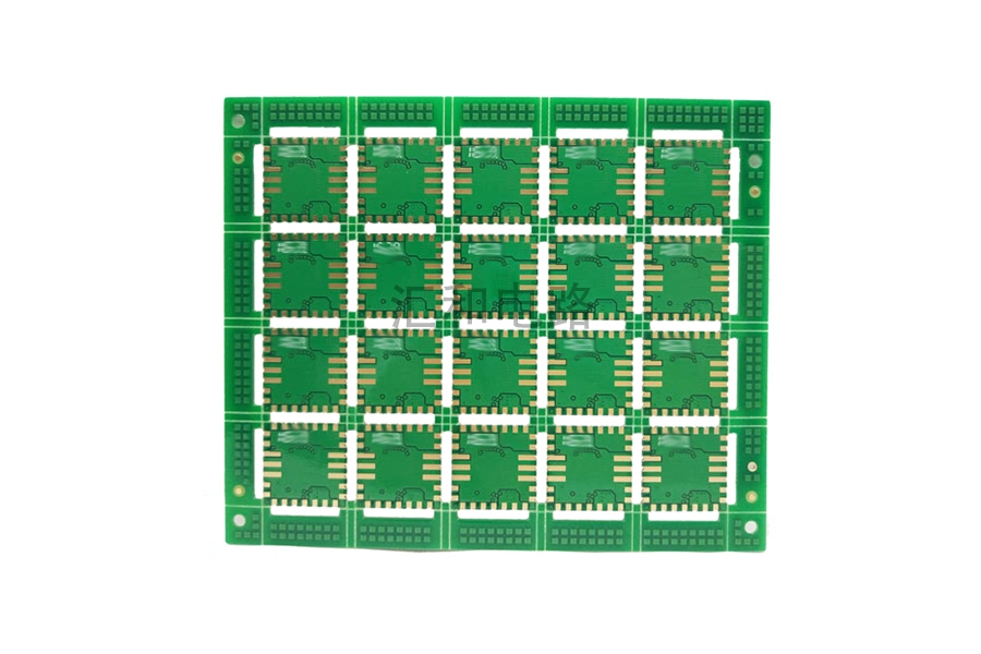
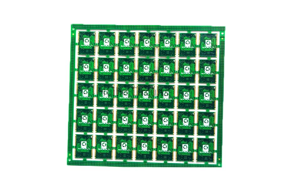
Product detail pictures:


Related Product Guide:
We take "customer-friendly, quality-oriented, integrative, innovative" as objectives. "Truth and honesty" is our administration ideal for China Wholesale Pcb Via In Pad Factories - 2 Layer ENIG Heavy Copper PCB – Huihe , The product will supply to all over the world, such as: Bangladesh, Johannesburg, United States, "Make the women more attractive "is our sales philosophy. "Being customers' trusted and preferred brand supplier" is the goal of our company. We are strict with every part of our work. We sincerely welcome friends to negotiate business and start cooperation. We hope to join hands with friends in different industries to create a brilliant future.
Staff is skilled, well-equipped, process is specification, products meet the requirements and delivery is guaranteed, a best partner!
-
Cheapest Factory Rohs Pcb Board Quotes - 8 Lay...
-
China Wholesale Power Supply Pcb Board Factorie...
-
China Wholesale Mosfet Pcb Factories - 4 Layer...
-

China Wholesale Ic Circuit Board Suppliers - ...
-

China Wholesale Electric Circuit Board Pricelis...
-
China Wholesale Lcd Pcb Board Pricelist - 6 la...


