
China Wholesale Pcb Service Factories - 8 Layer ENIG via-in-pad PCB – Huihe
China Wholesale Pcb Service Factories - 8 Layer ENIG via-in-pad PCB – Huihe Detail:
The most difficult thing to control the plug hole in the via-in-pad is the solder ball or pad on the ink in the hole. Due to the necessity of using high density BGA (ball grid array) and the miniaturization of SMD chip, the application of in tray hole technology is more and more. Through the reliable through hole filling process, the in plate hole technology can be applied to the design and manufacture of high-density multilayer board, and avoid abnormal welding. Huihe Circuits has been using via-in-pad technology for many years, and has an efficient and reliable production process.
Parameters of via-in-pad
|
|
Conventional products |
Special products |
Special products |
|
Hole filling standard |
IPC 4761 Type VII |
IPC 4761 Type VII |
- |
|
Min Hole Diameter |
200µm |
150µm |
100µm |
|
Minimum pad size |
400µm |
350µm |
300µm |
|
Max Hole Diameter |
500µm |
400µm |
- |
|
Maximum pad size |
700µm |
600µm |
- |
|
Minimum pin pitch |
600µm |
550µm |
500µm |
|
Aspect Ratio:Conventional via |
1:12 |
1:12 |
1:10 |
|
Aspect Ratio:Blind via |
1:1 |
1:1 |
1:1 |
Function of plug hole
1.Prevent the tin from passing through the conduction hole through the component surface during wave soldering
2.Avoid flux residue in the through-hole
3.Prevent tin balls from popping out during wave soldering, resulting in short circuit
4.Prevent the surface solder paste from flowing into the hole, causing virtual welding and affecting the fitting
Advantages of via-in-pad
1.Improve heat dissipation
2.The voltage withstand capacity of vias is improved
3.Provide a flat and consistent surface
4.Lower parasitic inductance
Our advantage
1. Own factory, factory area 12000 square meters, factory direct sales
2. The marketing team provides fast and high-quality pre-sales and after-sales services
3.Process-based processing of PCB design data to ensure that customers can review and confirm in the first time
Equipment display

Automatic Plating Line

PTH line

LDI

CCD Exposure Machine
Application

Communications

Security electronics

Railtransit
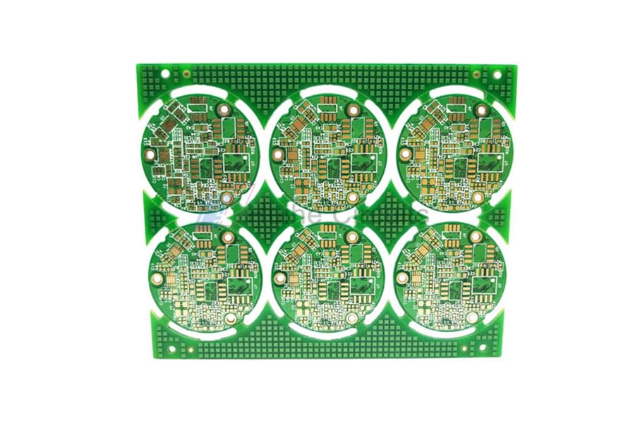
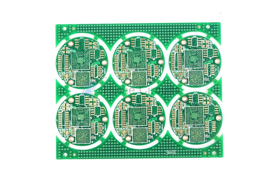
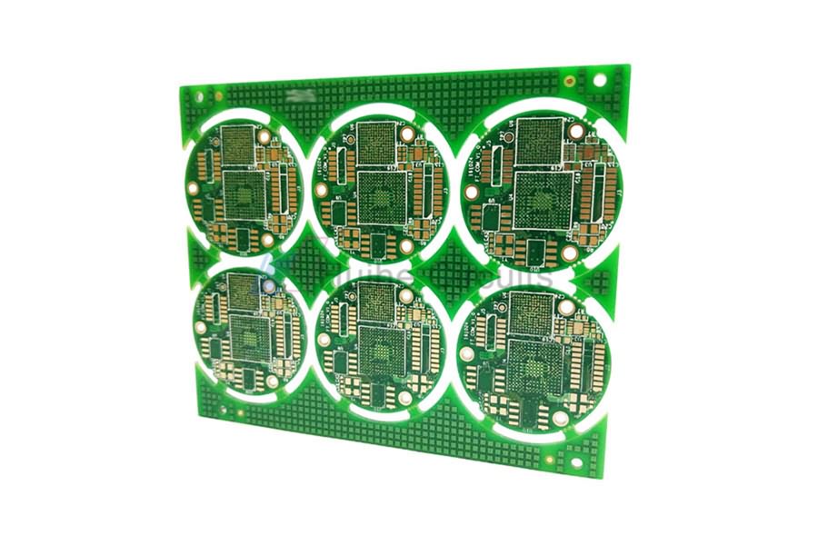
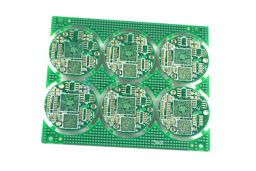
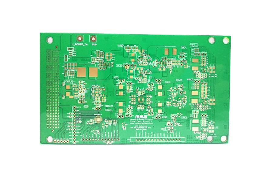
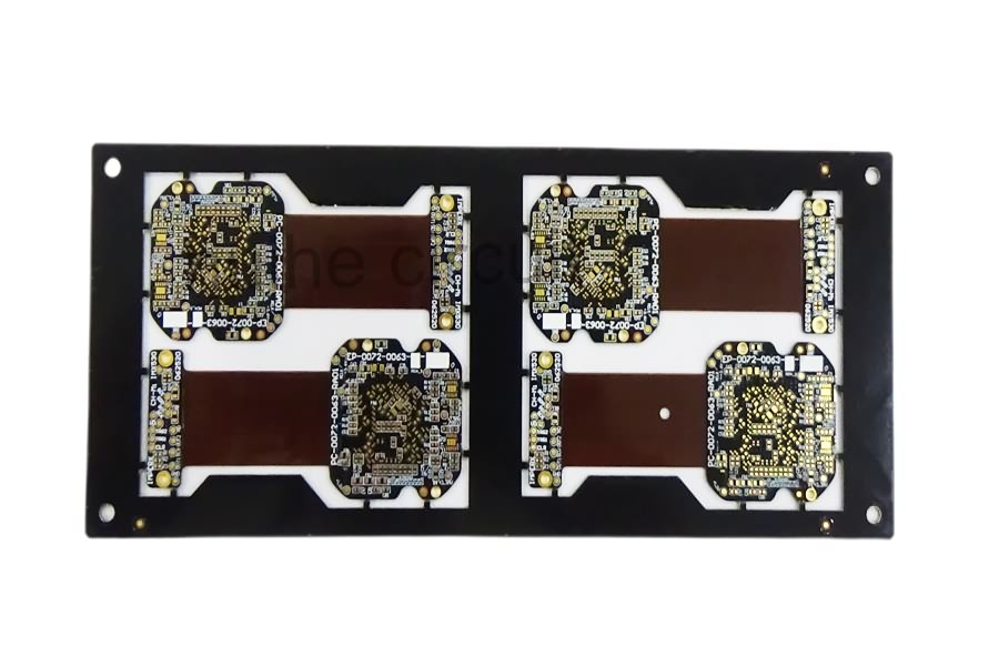
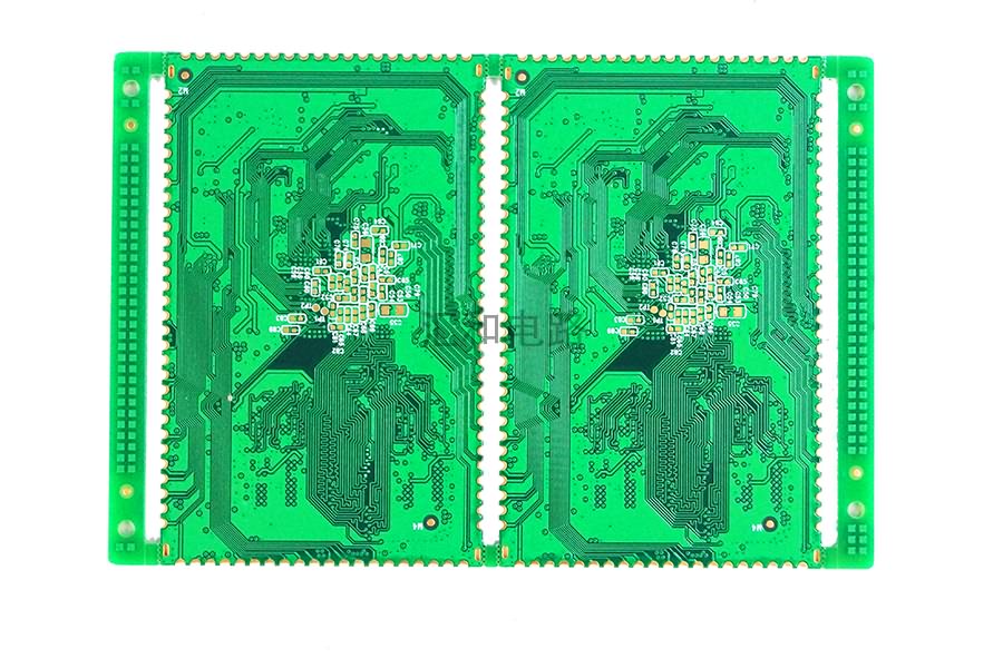
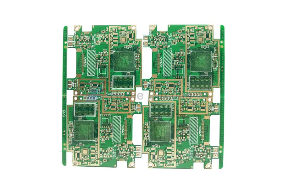
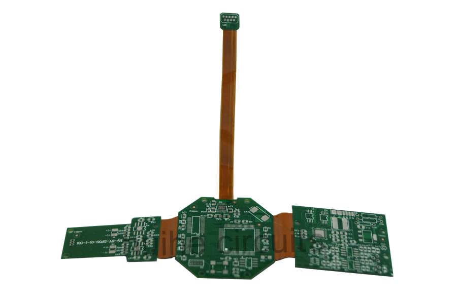
Product detail pictures:
Related Product Guide:
Sticking to your belief of "Creating solutions of high quality and generating buddies with people from all around the world", we always put the fascination of customers to start with for China Wholesale Pcb Service Factories - 8 Layer ENIG via-in-pad PCB – Huihe , The product will supply to all over the world, such as: Cambodia, Johor, Singapore, Our continual availability of high grade products in combination with our excellent pre-sale and after-sales service ensures strong competitiveness in an increasingly globalized market. welcome new and old customers from all walks of life to contact us for future business relationships and mutual success!
The product manager is a very hot and professional person, we have a pleasant conversation, and finally we reached a consensus agreement.
-
China Wholesale Fast Pcb Prototyping Suppliers ...
-
China Manufacturer for China Double Side Pcb -...
-
China Wholesale Small Prototype Board Pricelist...
-
China Wholesale High Speed Pcb Suppliers - 8 L...
-
China Wholesale Ic Pcb Board Manufacturers - 8...
-
China Wholesale Automatic Stabilizer Circuit Bo...


