
China Wholesale Pcb Prototype Services Factories - 6 Layer ENIG Via-In-Pad PCB – Huihe
China Wholesale Pcb Prototype Services Factories - 6 Layer ENIG Via-In-Pad PCB – Huihe Detail:
Function Of Plug Hole
The plug hole program of printed circuit board (PCB) is a process produced by the higher requirements of PCB manufacturing process and surface mount technology:
1.Avoid short circuit caused by tin penetrating through the component surface from the through hole during PCB over wave soldering.
2.Avoid flux remaining in the through hole.
3.Prevent solder bead from popping out during over wave soldering, resulting in short circuit.
4.Prevent the surface solder paste from flowing into the hole, causing false soldering and affecting the mounting.
Via In pad Process
Ddefine
For the holes of some small parts to be welded on the ordinary PCB , the traditional production method is to drill a hole on the board, and then coat a layer of copper in the hole to realize the conduction between layers, and then lead a wire to connect a welding pad to complete the welding with the outside parts.
Development
The Via in Pad manufacturing process is being developed against the backdrop of increasingly dense, interconnected circuit boards, where there is no more room for the wires and pads that connect the through holes.
Fuction
The production process of VIA IN PAD makes the PCB production process three-dimensional, effectively saves the horizontal space, and ADAPTS to the development trend of modern circuit board with high density and interconnection.
Factory Show

PCB Manufacturing Base

Admin Receptionist

Meeting Room

General Office
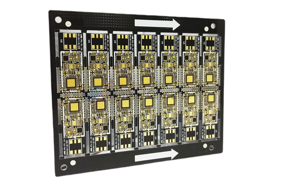
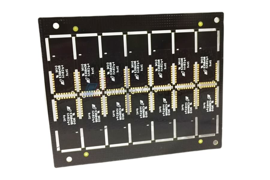
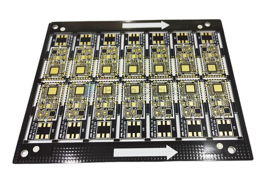
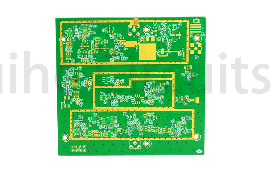
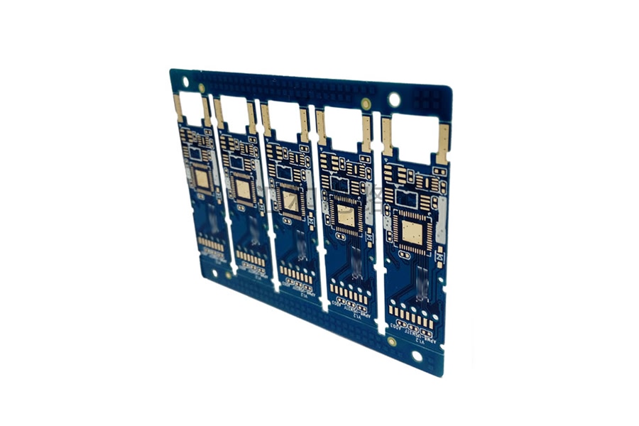
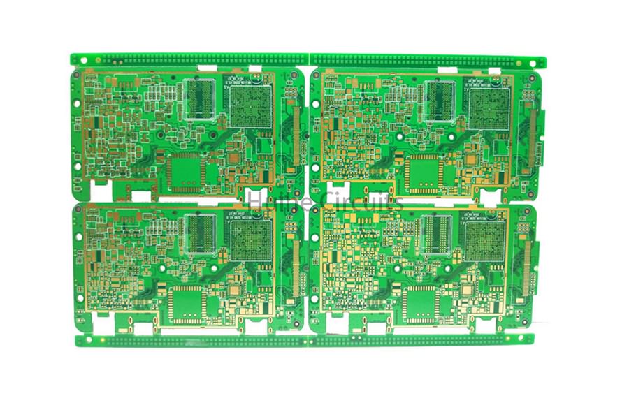
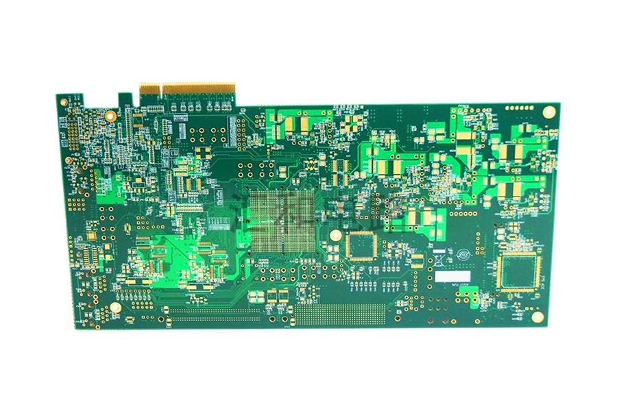
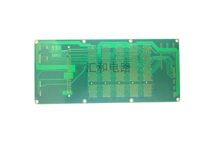
Product detail pictures:

Related Product Guide:
Our business aims to operating faithfully, serving to all of our clients , and working in new technology and new machine continuously for China Wholesale Pcb Prototype Services Factories - 6 Layer ENIG Via-In-Pad PCB – Huihe , The product will supply to all over the world, such as: Malta, Germany, California, With the technology as the core, develop and produce high-quality products according to the diverse needs of the market. With this concept,the company will continue to develop products with high added values and continuously improve products,and will provide many customers with the best products and services!
The goods we received and the sample sales staff display to us have the same quality, it is really a creditable manufacturer.
-
China Wholesale Pcb Assembly Manufacturers - 6...
-
China Wholesale Pwb Printed Wiring Board Suppli...
-
China Wholesale Double Sided Pcb Board Prototyp...
-
China Wholesale Stabilizer Pcb Board Suppliers ...
-
China Wholesale Teflon Pcb Board Quotes - 6 La...
-

China Wholesale Pcba Quotes - 14 Layer High TG...


