
China Wholesale Pcb Custom Order Factories - 14 Layer Blind Buried Via PCB – Huihe
China Wholesale Pcb Custom Order Factories - 14 Layer Blind Buried Via PCB – Huihe Detail:
About Blind Buried Via PCB
Blind vias and buried vias are two ways to establish connections between layers of printed circuit board. The blind vias of the printed circuit board are copper-plated vias that can be connected to the outer layer through most of the inner layer. The burrow connects two or more inner layers but does not penetrate the outer layer. Use microblind vias to increase line distribution density, improve radio frequency and electromagnetic interference, heat conduction, applied to servers, mobile phones, digital cameras.
Buried Vias PCB
The buried Vias connects two or more inner layers but does not penetrate the outer layer
|
Min Hole Diameter/mm |
Min ring/mm |
via-in-pad Diameter/mm |
Maximum Diameter/mm |
Aspect Ratio |
|
|
Blind Vias(conventional) |
0.1 |
0.1 |
0.3 |
0.4 |
1:10 |
|
Blind Vias(special product) |
0.075 |
0.075 |
0.225 |
0.4 |
1:12 |
Blind Vias PCB
Blind Vias is to connect an outer layer to at least one inner layer
|
|
Min. Hole Diameter/mm |
Minimum ring/mm |
via-in-pad Diameter/mm |
Maximum Diameter/mm |
Aspect Ratio |
|
Blind Vias(mechanical drilling) |
0.1 |
0.1 |
0.3 |
0.4 |
1:10 |
|
Blind Vias(Laser drilling) |
0.075 |
0.075 |
0.225 |
0.4 |
1:12 |
The advantage of blind Vias and buried Vias for engineers is the increase of component density without increasing layer number and size of circuit board. For electronic products with narrow space and small design tolerance, blind hole design is a good choice. The use of such holes helps the circuit design engineer to design a reasonable hole/pad ratio to avoid excessive ratios.
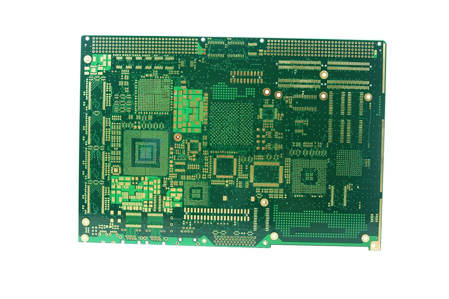
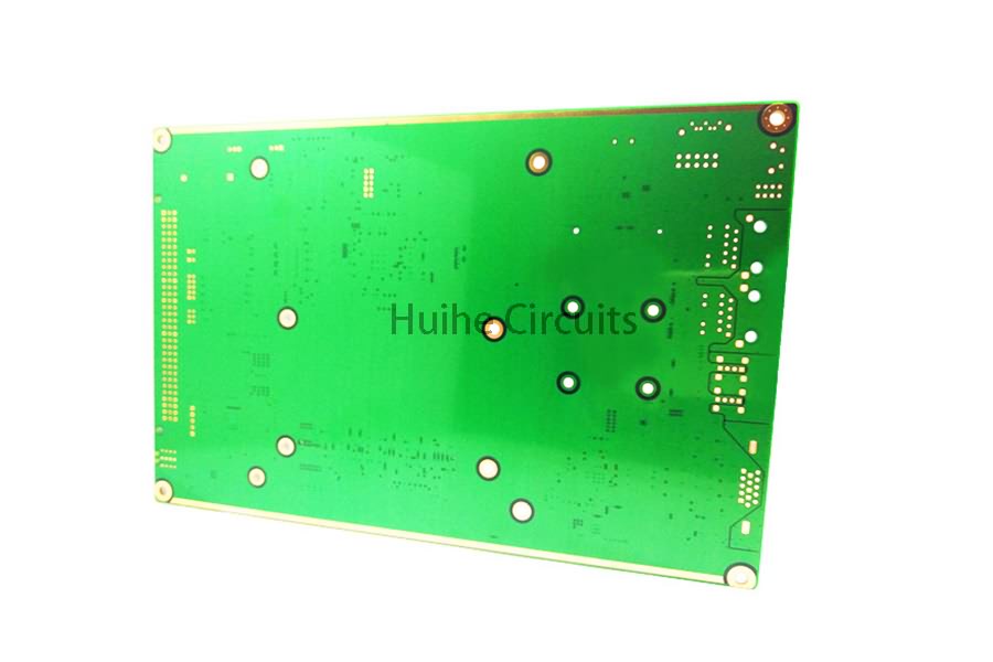
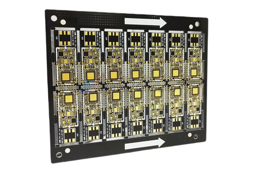
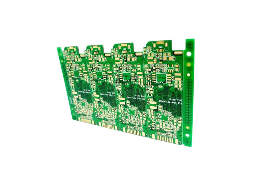
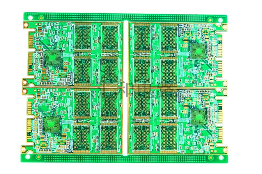
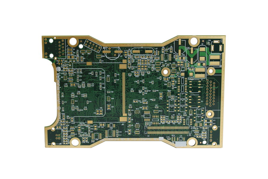
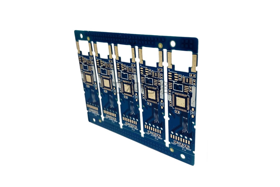
Product detail pictures:


Related Product Guide:
Our well-equipped facilities and great good quality regulate throughout all stages of manufacturing enables us to guarantee total buyer gratification for China Wholesale Pcb Custom Order Factories - 14 Layer Blind Buried Via PCB – Huihe , The product will supply to all over the world, such as: Paraguay, St. Petersburg, Monaco, We have developed large markets in many countries, such as Europe and the United States, Eastern Europe and Eastern Asia. Meanwhile with the powerful predominance in persons with ability, strict production management and business concept.we constantly carry on self-innovation, technological innovation, managing innovation and business concept innovation. To follow the world markets fashion, new products are kept on researching and providing to guarantee our competitive advantage in styles, quality, price and service.
Customer service staff and sales man are very patience and they all good at English, product's arrival is also very timely, a good supplier.
-
China Wholesale Flexible Pcb Fabrication Quotes...
-
China Wholesale Double Sided Pcb Manufacturers ...
-
China Wholesale Flexible Pcb Fabrication Manufa...
-
China Wholesale Matte Black Pcb Suppliers - 8 ...
-
Free sample for Led Pcb Board Price - 10 Layer...
-
China Wholesale Pcb Stripboard Quotes - 4 Laye...


