
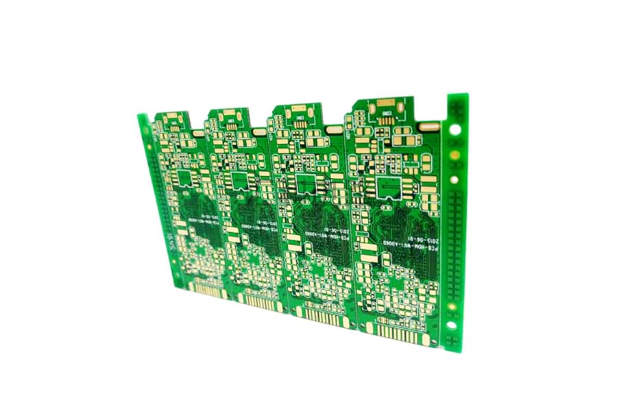
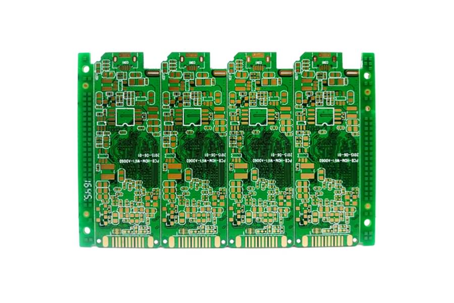
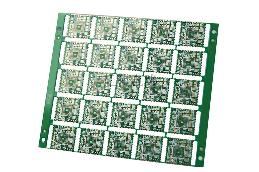
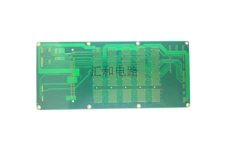
China Wholesale Pcb Assembly Services Factories - 6 Layer ENIG Impedance Control PCB – Huihe
China Wholesale Pcb Assembly Services Factories - 6 Layer ENIG Impedance Control PCB – Huihe Detail:
Difference Between Pad And Via
1. Definitions Differ
Pad: is the basic unit of surface mount assembly, which is used to form the landpattern of the circuit board, that is, a variety of combinations of pads designed for special component types.
Through hole: through hole is also called metallization hole. In the double panel and multilayer PCB, a common hole is drilled at the junction of the wires that need to be connected between the layers in order to connect the printed wires between layers. The main parameters of the hole are the outer diameter of the hole and the size of the hole.
The hole itself has parasitic capacitance and inductance to the ground, which often brings great negative effect to the circuit design.
2. Different Principles
Pad: When a pad structure is not designed correctly, it is difficult to reach the desired weld point. Can be used for surface-mounted components or for plug-in components.
Through hole: In a circuit board, a line jumps from one side of the board to the other. The hole connecting the two wires is also called a hole (as opposed to a pad, there is no solder layer on the side). Also known as metallization hole, in the double panel and multilayer PCB, for connecting the printed wire between the layers, in each layer need to be connected at the intersection of the wire drilling on a public hole, that is, through the hole.
Technically, a layer of metal is PCB on the cylindrical surface of the hole wall of the hole through the chemical deposition method to connect the copper foil that needs to be connected in the middle layer, and the upper and lower sides of the hole through the shape of a circular solder pad, the parameters of the hole mainly include the outer diameter of the hole and the size of the hole.
3. Different Effects
Through hole: the hole on PCB, play the role of conduction or heat dissipation.
Pad: it is the copper plate of PCB, some cooperate with the hole to connect, and some square plate, mainly used to paste parts.
Equipment Display

PCB Automatic Plating Line

PCB PTH Line

PCB LDI

PCB CCD Exposure Machine
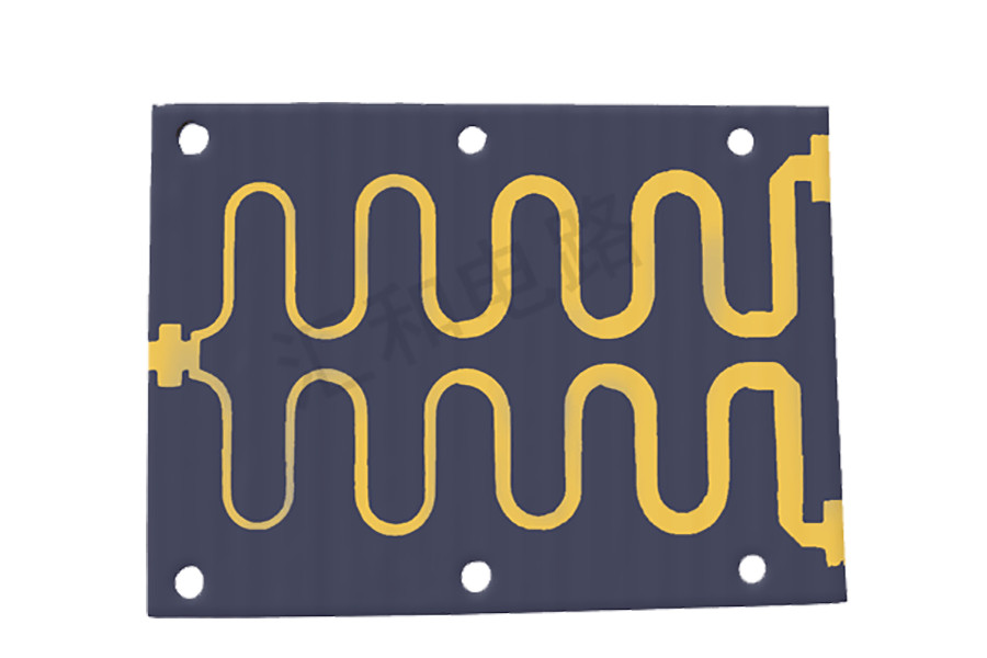
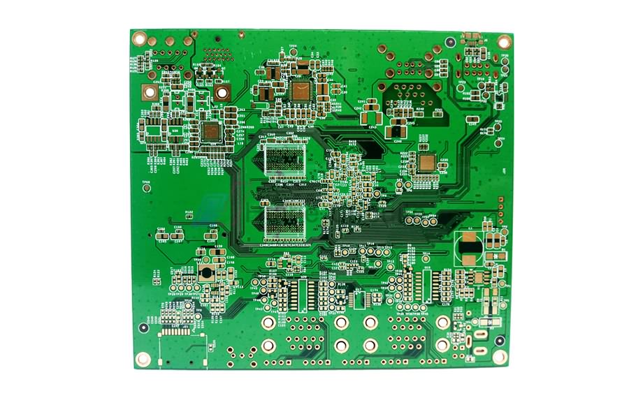
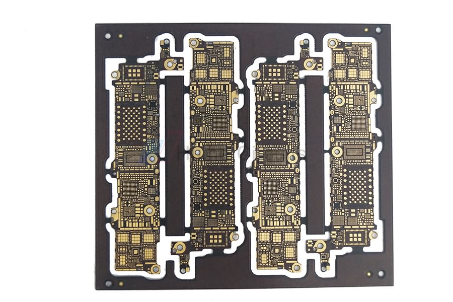
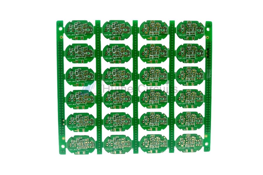
Product detail pictures:


Related Product Guide:
We've got a really efficient group to deal with inquiries from prospects. Our purpose is "100% customer fulfillment by our product excellent, price & our group service" and enjoy a superb track record amid clientele. With many factories, we can easily deliver a wide selection of China Wholesale Pcb Assembly Services Factories - 6 Layer ENIG Impedance Control PCB – Huihe , The product will supply to all over the world, such as: Thailand, moldova, French, Satisfaction and good credit to every customer is our priority. We focus on every detail of order processing for customers till they have received safe and sound solutions with good logistics service and economical cost. Depending on this, our solutions are sold very well in the countries in Africa, the Mid-East and Southeast Asia.
Production management mechanism is completed, quality is guaranteed, high credibility and service let the cooperation is easy, perfect!
-
China Wholesale Flex Pcb Prototyping Factories ...
-
China Wholesale Eft Printed Circuit Board Price...
-
China Wholesale Bass Filter Circuit Board Facto...
-
China Wholesale Rohs Circuit Board Manufacturer...
-
China Wholesale Cpu Pcb Suppliers - 8 Layer EN...
-
2022 China New Design Rigid Flex Pcb Quotes - ...


