
China Wholesale Non Printed Circuit Board Pricelist - 16 Layer ENIG Press Fit Hole PCB 31525 – Huihe
China Wholesale Non Printed Circuit Board Pricelist - 16 Layer ENIG Press Fit Hole PCB 31525 – Huihe Detail:
About Via-In-Pad PCB
The Via-In-Pad PCBs are generally blind holes, which are mainly used to connect the inner layer or the secondary outer layer of HDI PCB with the outer layer, so as to improve the electrical performance and reliability of electronic products, shorten the signal transmission wire, reduce the inductive reactance and capacitive reactance of the transmission line, as well as the internal and external electromagnetic interference.
It’s used for conducting. The main problem of plug holes in the PCB industry is oil leakage from plug holes, which can be said to be a persistent disease in the industry. It seriously affects the production quality, delivery time and efficiency of PCB. At present, most high-end dense PCBs have this kind of design. Therefore, PCB industry urgently needs to solve the problem of oil leakage from plug holes
Main factors of oil emission from via in pad plug hole
Spacing between plug hole and pad: in the actual PCB anti-welding production process, except the plate hole is easy to escape. Other plug hole and window spacing is less than 0.1mm 4mil) and plug hole and anti-soldering window tangential, intersection plate is also easy to exist after curing oil leakage;
PCB thickness and aperture: plate thickness and aperture are positively correlated with the degree and proportion of oil emission;
Parallelic film design: when the Via-In-Pad PCB or the small spacing hole intersects the pad, the parallelic film will generally design the light transmittance point at the window position (to expose the ink in the hole) “to avoid the ink in the hole seeping into the pad during development, but the light transmittance design is too small to achieve the effect of exposure, and the light transmittance point is too large to easily cause the offset. Produces green oil on the PAD.
Curing conditions: because the design of the translucent point of the Via-In-Pad PCB to the film should be smaller than the hole, the part of the ink in the hole is greater than the translucent point when exposed is not exposed to light. Ink is not photosensitive curing, development after the general need to reverse exposure or UV once, in order to cure the ink here. A layer of curing film is formed on the surface of the hole to prevent thermal expansion of ink in the hole after curing. After curing, the longer the time of the low temperature section, and the lower the temperature of the low temperature section, the smaller the proportion and degree of oil emission;
Plugging ink: different manufacturers of ink formula different quality effect will also have a certain difference
Equipment display

Automatic Plating Line

PTH line

LDI

CCD Exposure Machine
Application

Communications

Security electronics

Railtransit
Our factory


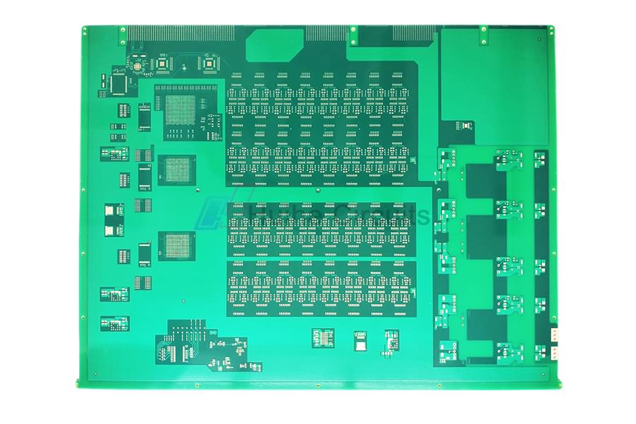
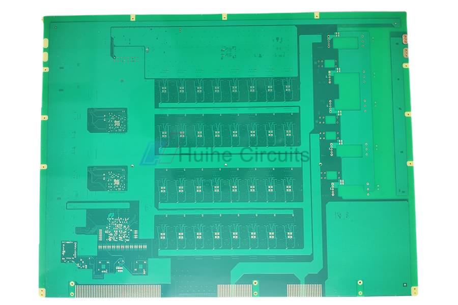
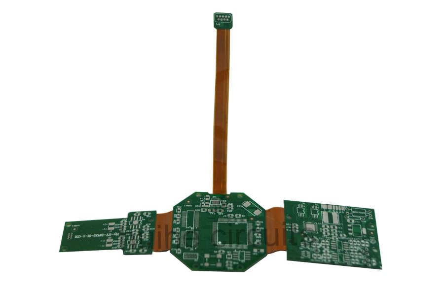
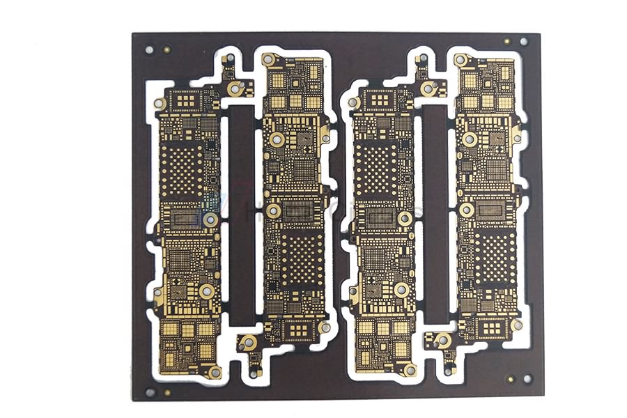
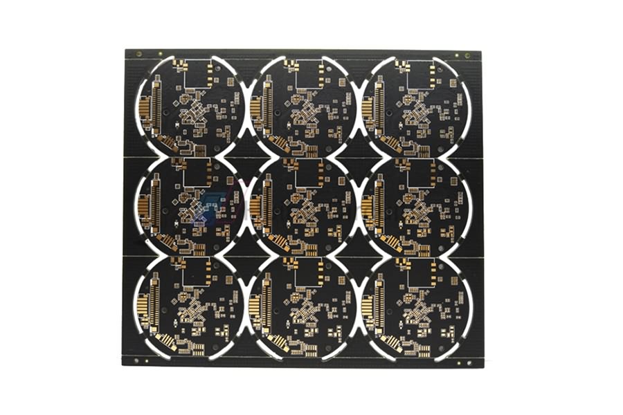
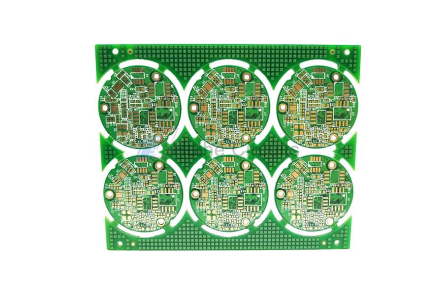
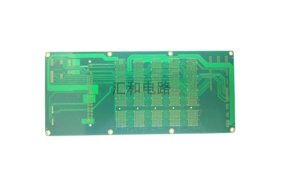
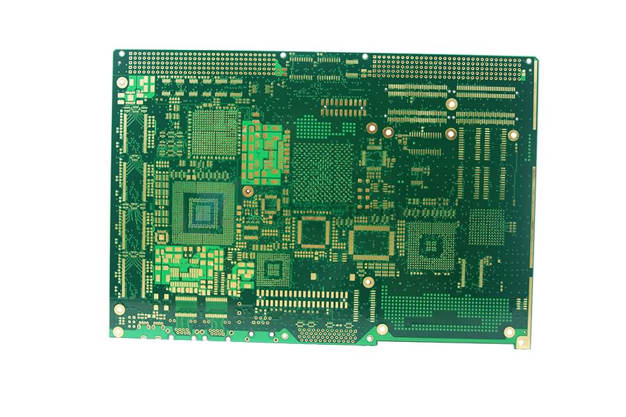
Product detail pictures:
Related Product Guide:
High quality Initial,and Buyer Supreme is our guideline to offer the ideal assistance to our shoppers.At present, we are striving our best to become amongst the ideal exporters inside our industry to satisfy shoppers more want for China Wholesale Non Printed Circuit Board Pricelist - 16 Layer ENIG Press Fit Hole PCB 31525 – Huihe , The product will supply to all over the world, such as: Senegal, Bandung, Tunisia, We welcome you to visit our company, factory and our showroom displayed various products that will meet your expectation, meanwhile, it is convenient to visit our website, our sales staff will try their efforts to offer you the best service. If you need to have more information, remember to do not hesitate to contact us by E-mail or telephone.
Goods just received, we are very satisfied, a very good supplier, hope to make persistent efforts to do better.
-
China Wholesale Soldering Pcb Components Manufa...
-
Best Price for Flexible Printed Circuit Board M...
-
China Wholesale Best Pcb Factories - 6 layer E...
-
High Quality Flexible Circuit Suppliers - 8 La...
-
China Wholesale Motion Sensor Circuit Board Quo...
-
China Wholesale Flexible Circuit Board Supplier...


