
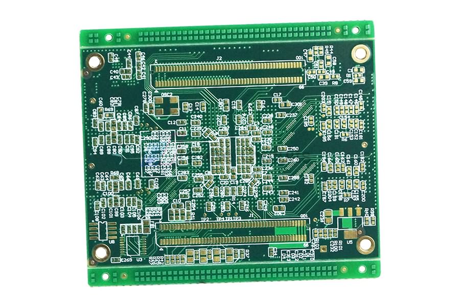
China Wholesale Mosfet Pcb Factories - 6 Layer ENIG Blind Vias PCB – Huihe
China Wholesale Mosfet Pcb Factories - 6 Layer ENIG Blind Vias PCB – Huihe Detail:
Features Of The Blind Via PCB
Blind Vias are located on the top and bottom surfaces of the circuit board and have a certain depth for the connection between the surface circuit and the inner circuit below. The depth of the hole usually does not exceed a certain ratio (aperture). This way of production will need to pay special attention to the depth of the hole (the Z axis) to the right, do not pay attention to words will cause difficult hole plating so almost no factory used, can also be connected in advance to the layer in the individual circuit when the circuit was first drill hole, and then sticking up, need more precision positioning and contrapuntal device.
Advantage Of The Blind Buried Via PCB
The advantage of blind buried vias PCB for engineers is that the density of components is increased, while the number of layers and size of circuit board are not increased. For electronic products with narrow space and small design tolerance, blind hole design is a good choice. The use of this kind of hole is helpful for circuit design engineers to design reasonable hole/pad ratio and avoid excessive ratio.
Equipment Display

PCB Automatic Plating Line

PCB PTH Line

PCB LDI

PCB CCD Exposure Machine
Factory Show

PCB Manufacturing Base

Admin Receptionist

Meeting Room

General Office
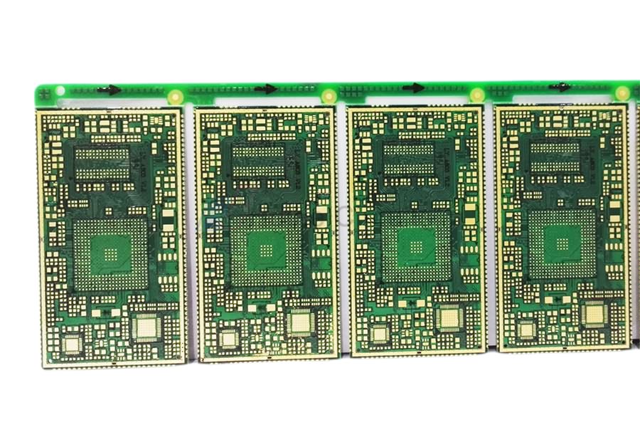
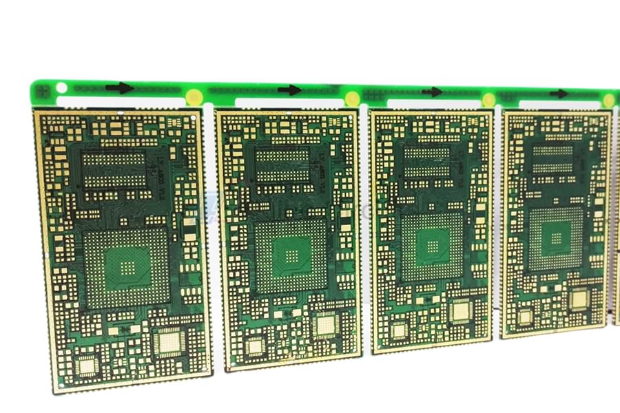
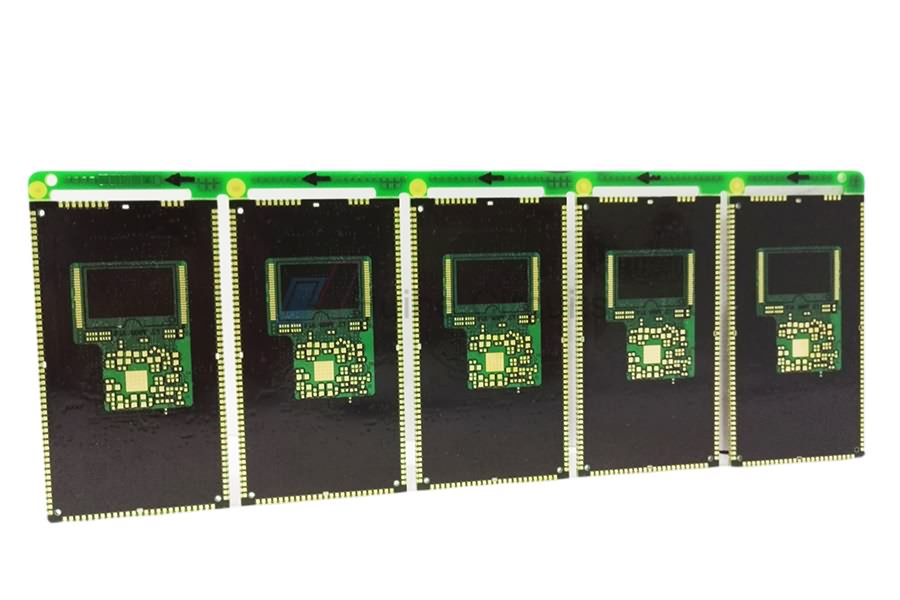
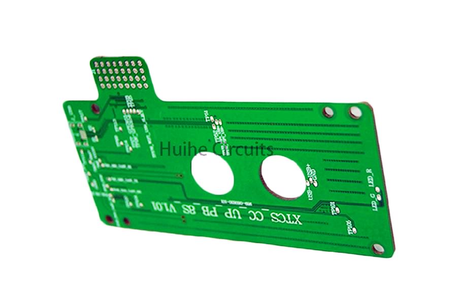
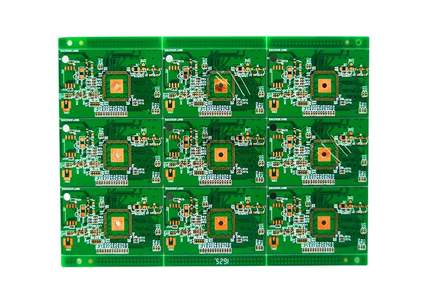
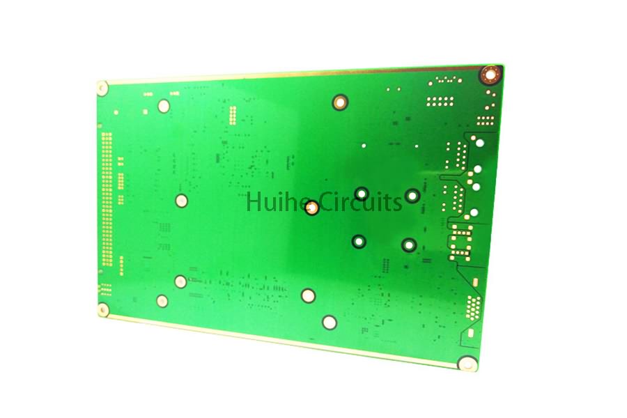
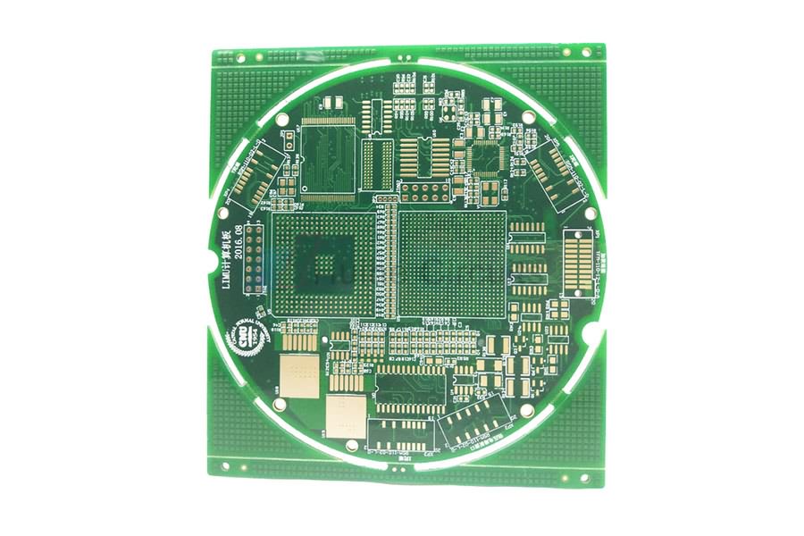
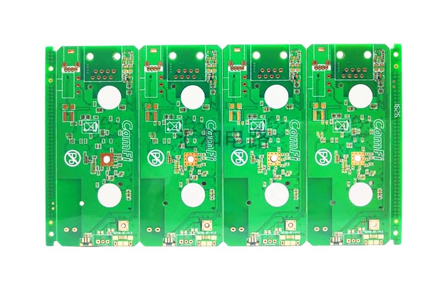
Product detail pictures:
Related Product Guide:
Our pursuit and firm aim should be to "Always fulfill our buyer requirements". We carry on to produce and structure top-quality excellent solutions for equally our aged and new consumers and accomplish a win-win prospect for our consumers as well as us for China Wholesale Mosfet Pcb Factories - 6 Layer ENIG Blind Vias PCB – Huihe , The product will supply to all over the world, such as: Wellington, Ukraine, Hamburg, We put the product quality and customer's benefits to the first place. Our experienced salesmen supply prompt and efficient service. Quality control group make sure the best quality. We believe quality comes from detail. If you have demand, allow us to work together to get success.
As an international trading company, we have numerous partners, but about your company, I just want to say, you are really good, wide range, good quality, reasonable prices, warm and thoughtful service, advanced technology and equipment and workers have professional training, feedback and product update is timely, in short, this is a very pleasant cooperation, and we look forward to the next cooperation!
-
China Wholesale Pcba Quotes - 10 Layer ENIG Im...
-
China Wholesale Custom Pcb Manufacturers - 4 L...
-
China Wholesale High Current Pcb Pricelist - 6...
-
China Wholesale Pwb Printed Wiring Board Pricel...
-
Good Wholesale Vendors Pcb Circuit Board - 4 L...
-
China Wholesale Timer Circuit Board Pricelist -...


