China Wholesale Hitech Pcb Suppliers - 6 Layer HASL Blind Buried Via PCB – Huihe
China Wholesale Hitech Pcb Suppliers - 6 Layer HASL Blind Buried Via PCB – Huihe Detail:
Features Of The Buried Via PCB
The manufacturing process cannot be achieved by drilling after bonding. Drilling must be performed at individual circuit layers. The inner layer must be partially bonded first, followed by electroplating treatment, and then all bonded finally. This process is usually used only on high-density PCBs to increase the available space for other circuit layers
The Basic Process Of HDI Blind Buried Via PCB
Equipment Display

PCB Automatic Plating Line

PCB PTH Line

PCB LDI

PCB CCD Exposure Machine
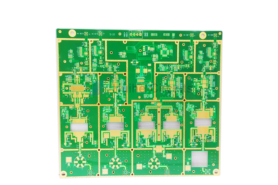
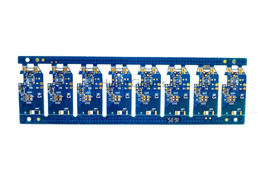
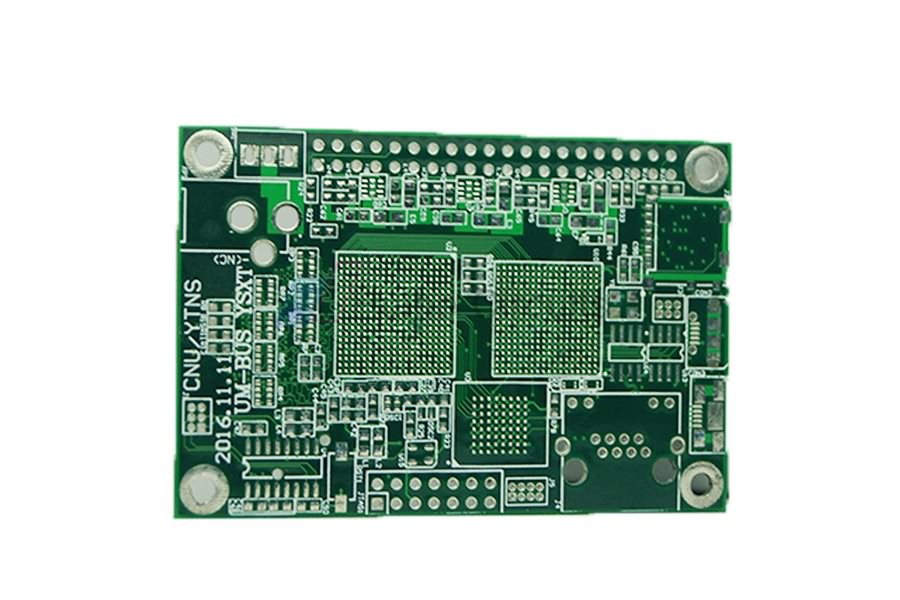
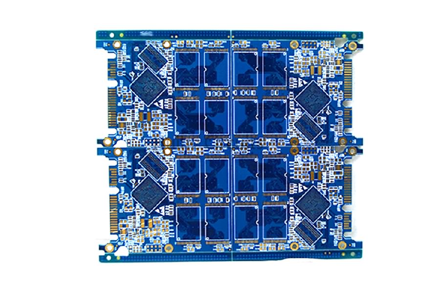
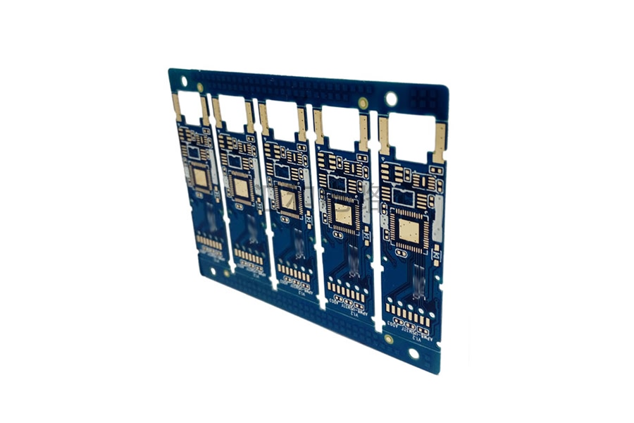
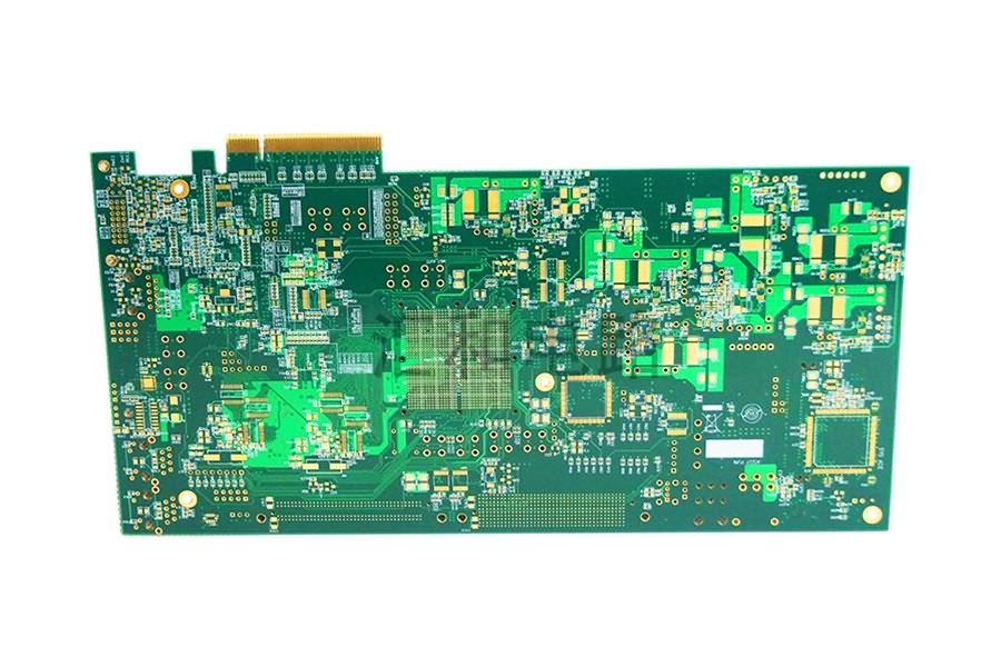
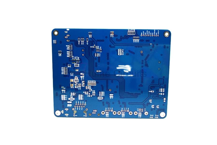
Product detail pictures:


Related Product Guide:
We often persist with the theory "Quality To start with, Prestige Supreme". We are fully committed to delivering our clientele with competitively priced good quality items, prompt delivery and experienced support for China Wholesale Hitech Pcb Suppliers - 6 Layer HASL Blind Buried Via PCB – Huihe , The product will supply to all over the world, such as: Swiss, Madagascar, Lesotho, We will supply much better products with diversified designs and professional services. We sincerely welcome friends from over the world to visit our company and cooperate with us on the basis of long-term and mutual benefits.
This manufacturer can keep improving and perfecting products and service, it is in line with the rules of market competition, a competitive company.
Write your message here and send it to us