China Wholesale Hitech Pcb Quotes - 14 Layer Blind Buried Via PCB – Huihe
China Wholesale Hitech Pcb Quotes - 14 Layer Blind Buried Via PCB – Huihe Detail:
About Blind Buried Via PCB
Blind vias and buried vias are two ways to establish connections between layers of printed circuit board. The blind vias of the printed circuit board are copper-plated vias that can be connected to the outer layer through most of the inner layer. The burrow connects two or more inner layers but does not penetrate the outer layer. Use microblind vias to increase line distribution density, improve radio frequency and electromagnetic interference, heat conduction, applied to servers, mobile phones, digital cameras.
Buried Vias PCB
The buried Vias connects two or more inner layers but does not penetrate the outer layer
|
Min Hole Diameter/mm |
Min ring/mm |
via-in-pad Diameter/mm |
Maximum Diameter/mm |
Aspect Ratio |
|
|
Blind Vias(conventional) |
0.1 |
0.1 |
0.3 |
0.4 |
1:10 |
|
Blind Vias(special product) |
0.075 |
0.075 |
0.225 |
0.4 |
1:12 |
Blind Vias PCB
Blind Vias is to connect an outer layer to at least one inner layer
|
|
Min. Hole Diameter/mm |
Minimum ring/mm |
via-in-pad Diameter/mm |
Maximum Diameter/mm |
Aspect Ratio |
|
Blind Vias(mechanical drilling) |
0.1 |
0.1 |
0.3 |
0.4 |
1:10 |
|
Blind Vias(Laser drilling) |
0.075 |
0.075 |
0.225 |
0.4 |
1:12 |
The advantage of blind Vias and buried Vias for engineers is the increase of component density without increasing layer number and size of circuit board. For electronic products with narrow space and small design tolerance, blind hole design is a good choice. The use of such holes helps the circuit design engineer to design a reasonable hole/pad ratio to avoid excessive ratios.
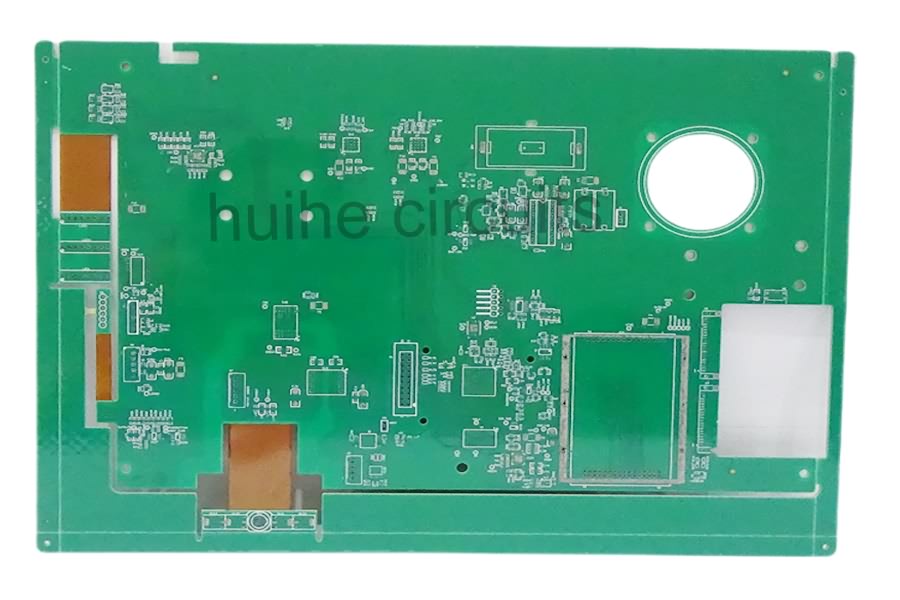
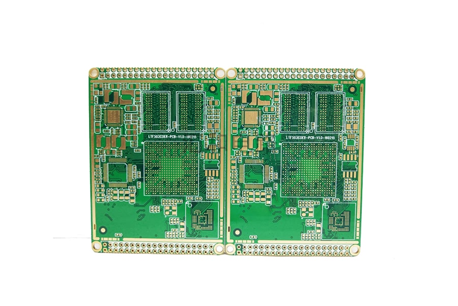
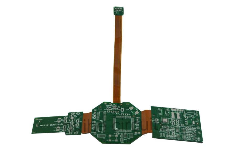
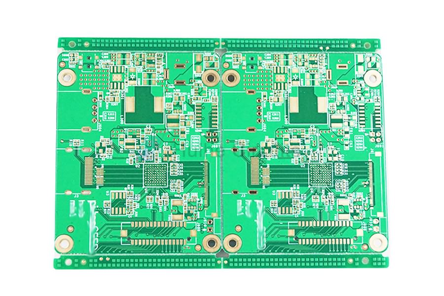
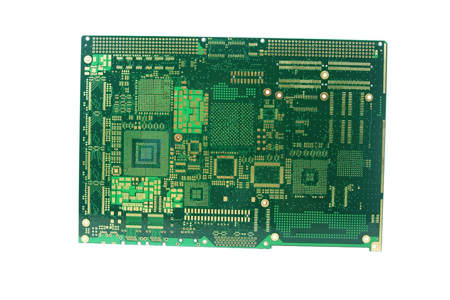
Product detail pictures:


Related Product Guide:
Reliable quality and good credit standing are our principles, which will help us at a top-ranking position. Adhering to the tenet of "quality first, customer supreme" for China Wholesale Hitech Pcb Quotes - 14 Layer Blind Buried Via PCB – Huihe , The product will supply to all over the world, such as: Kuala Lumpur, Bogota, Ireland, We are introduced as a one of the growing manufacture supplier and export of our products. We have a team of dedicated trained professional who take care the quality and timely supply. If you are looking for Good Quality at a good price and timely delivery. Do contact us.
The company keeps to the operation concept "scientific management, high quality and efficiency primacy, customer supreme", we have always maintained business cooperation. Work with you,we feel easy!