
China Wholesale Hitech Pcb Factories - 6 Layer ENIG Impedance Control Heavy Copper PCB – Huihe
China Wholesale Hitech Pcb Factories - 6 Layer ENIG Impedance Control Heavy Copper PCB – Huihe Detail:
Functions Of Heavy Copper PCB
Heavy copper PCB has the best extension functions, is not limited by the processing temperature, high melting point can be used oxygen blowing, low temperature at the same brittle and other hot melt welding, but also fire prevention, belongs to the non-combustible material. Even in highly corrosive atmospheric conditions, copper sheets form a strong, non-toxic passivation protective layer.
Difficulty In Machining Control Of Heavy Copper PCB
Thickness of copper PCB brings a series of processing difficulties to PCB processing, such as the need for multiple etching, insufficient pressing plate filling, drilling inner layer welding pad cracking, hole wall quality is difficult to guarantee and other problems.
1. Etching difficulties
With the increase of copper thickness, the side erosion will become more and more large due to the difficulty of exchange of potion.
2. Difficulty in laminating
(1) with the increase of copper thick, dark line clearance, under the same rate of residual copper, resin filling quantity should be increased, then you need to use more than one and a half curing to meet fill glue problem: because of the need to maximize the resin filling line clearance, in areas such as the rubber content is high, the resin curing liquid half piece do heavy copper laminate is the first choice. The semi-cured sheet is usually chosen for 1080 and 106. In the inner layer design, copper points and copper blocks are laid in the copper-free area or the final milling area to increase the residual copper rate and reduce the pressure of glue filling.
(2) The increase in the use of semi-solidified sheets will increase the risk of skateboards. The method of adding rivets can be adopted to strengthen the degree of fixation between core plates. As the copper thickness becomes larger and larger, resin is also used to fill the blank area between the graphs. Because the total copper thickness of the heavy copper PCB is generally more than 6oz, the CTE match between the materials is particularly important [such as copper CTE is 17ppm, fiberglass cloth is 6PPM-7ppm, resin is 0.02%. Therefore, in the process of PCB processing, the selection of fillers, low CTE and T high PCB is the basis to ensure the quality of heavy copper (power) PCB.
(3) As the thickness of copper and PCB increases, the more heat will be needed in lamination production. The actual heating rate will be slower, the actual duration of the high temperature section will be shorter, which will lead to insufficient resin curing of the semi-cured sheet, thus affecting the reliability of the plate; Therefore, it is necessary to increase the duration of the laminated high temperature section to ensure the curing effect of the semi-cured sheet. If the semi-cured sheet is insufficient, it leads to a large amount of glue removal relative to the core plate semi-cured sheet, and the formation of a ladder, and then the hole copper fracture due to the effect of stress.
Equipment Display

PCB Automatic Plating Line

PCB PTH Line

PCB LDI

PCB CCD Exposure Machine
Factory Show

PCB Manufacturing Base

Admin Receptionist

Meeting Room

General Office
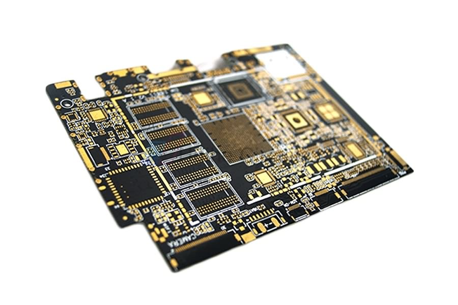
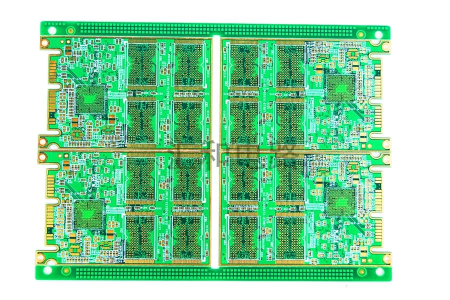
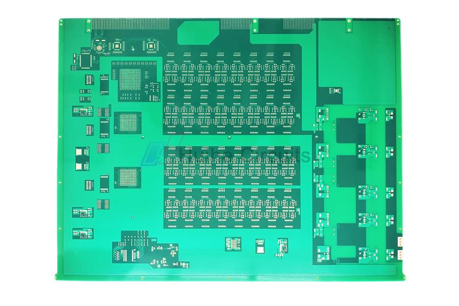
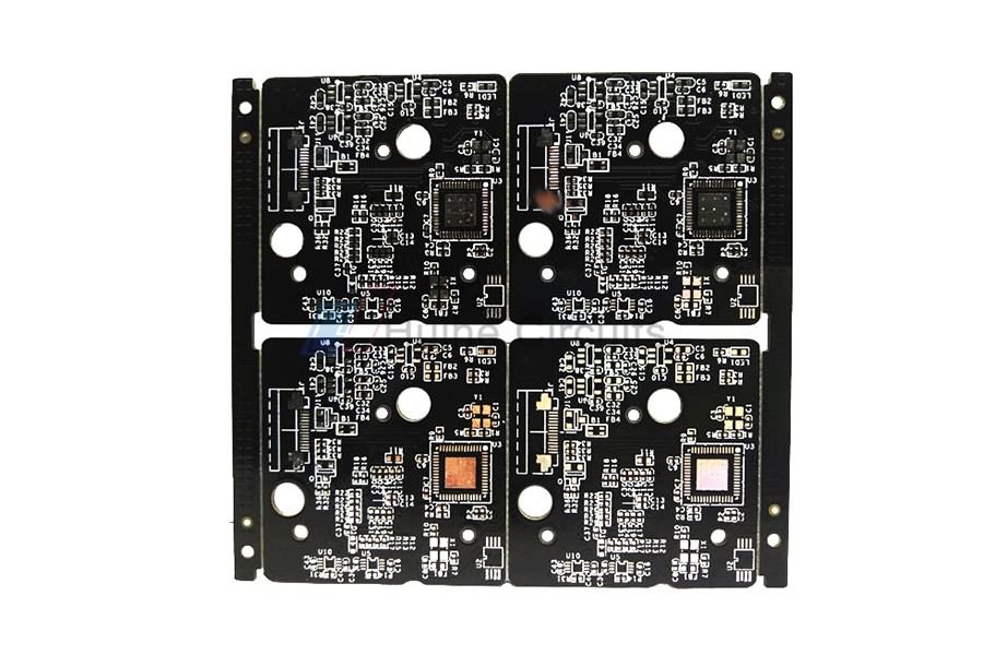
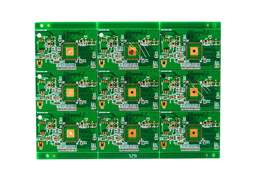
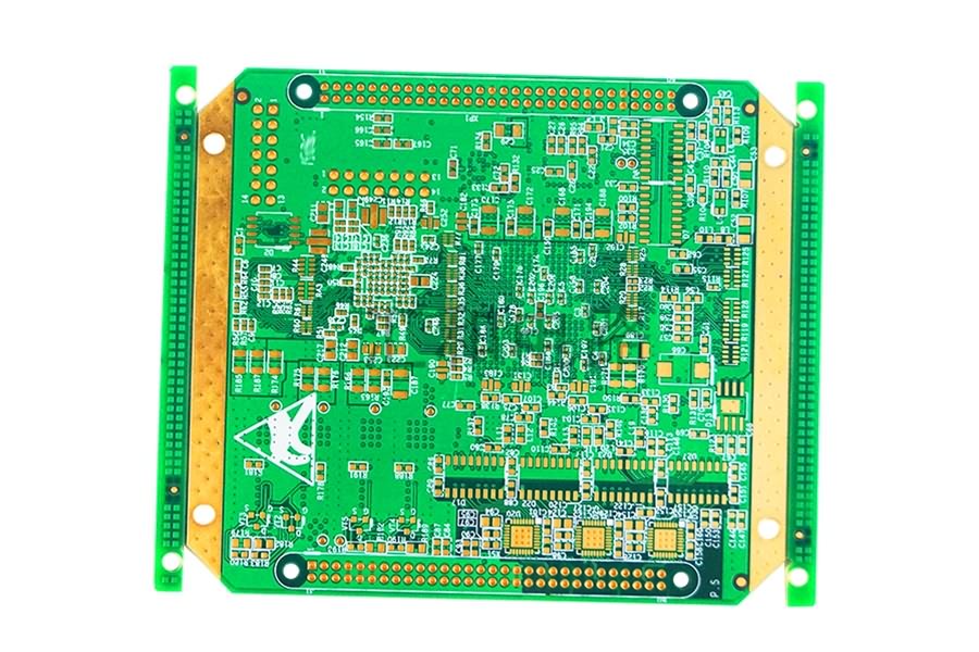
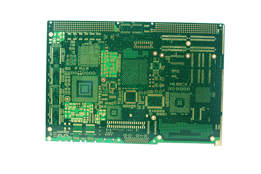
Product detail pictures:

Related Product Guide:
Our advancement depends over the superior machines, exceptional talents and continually strengthened technology forces for China Wholesale Hitech Pcb Factories - 6 Layer ENIG Impedance Control Heavy Copper PCB – Huihe , The product will supply to all over the world, such as: Canada, Norwegian, Ecuador, Our company has a skillful sales team, strong economic foundation, great technical force, advanced equipment, complete testing means, and excellent after-sales services. Our items have beautiful appearance, fine workmanship and superior quality and win the unanimous approvals of the customers all over the world.
As an international trading company, we have numerous partners, but about your company, I just want to say, you are really good, wide range, good quality, reasonable prices, warm and thoughtful service, advanced technology and equipment and workers have professional training, feedback and product update is timely, in short, this is a very pleasant cooperation, and we look forward to the next cooperation!
-
China wholesale Blinded And Buried Hole Pcb - ...
-
China Wholesale Bass Filter Circuit Board Facto...
-
Best-Selling 8layer Copper Pcb Board - 4 Layer...
-
China Wholesale Hitech Pcb Quotes - 4 Layer OS...
-
China Wholesale Pcb Making Factories - 16 Laye...
-
China Wholesale Order Custom Circuit Board Manu...


