
China Wholesale Glc Pcb Suppliers - 6 Layer HASL Blind Buried Via PCB 13699 – Huihe
China Wholesale Glc Pcb Suppliers - 6 Layer HASL Blind Buried Via PCB 13699 – Huihe Detail:
Features of the Buried Via
The manufacturing process cannot be achieved by drilling after bonding. Drilling must be performed at individual circuit layers. The inner layer must be partially bonded first, followed by electroplating treatment, and then all bonded finally. This process is usually used only on high-density PCBs to increase the available space for other circuit layers
The basic process of making HDI blind buried Via PCB
Equipment display

Automatic Plating Line

PTH line

LDI

CCD Exposure Machine
Application

Communications

Security electronics

Railtransit
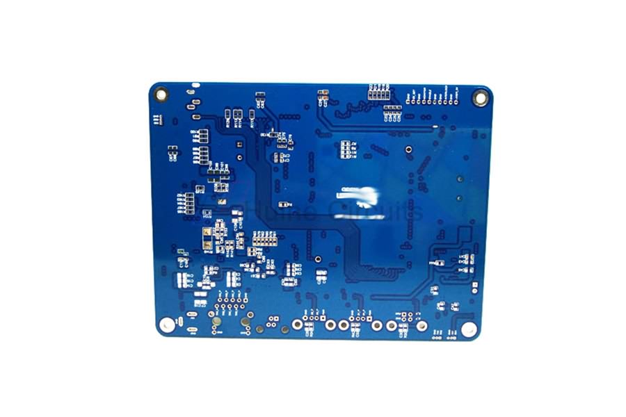
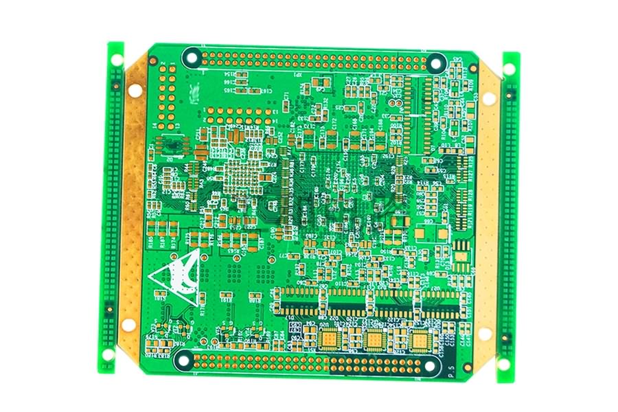
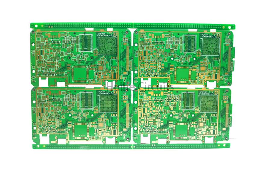
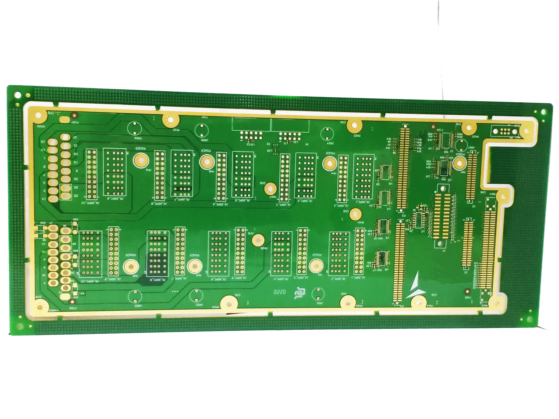
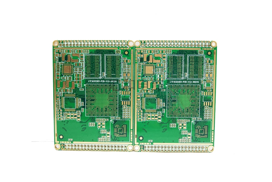
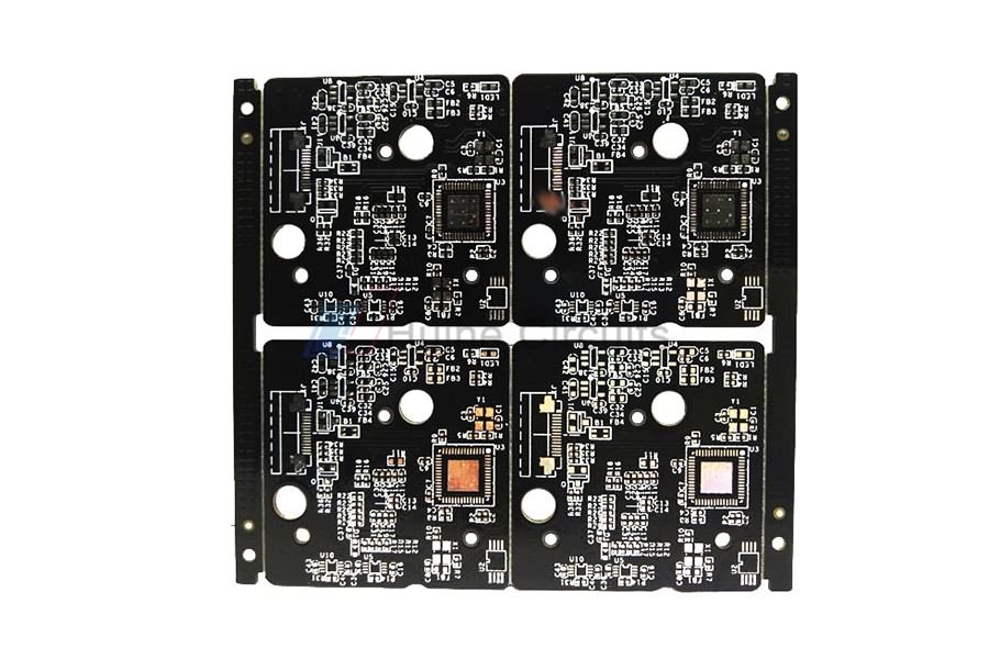
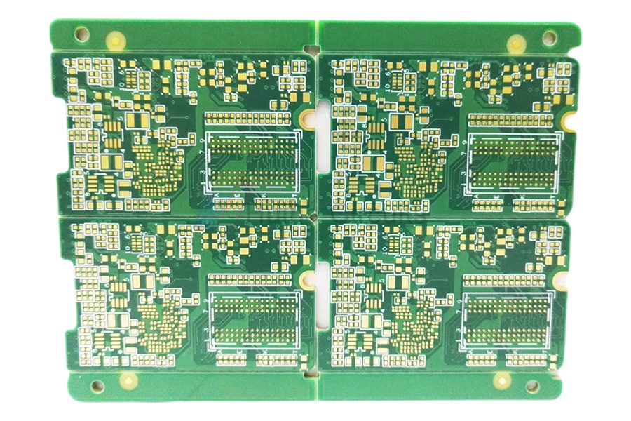
Product detail pictures:


Related Product Guide:
We've been proud with the significant shopper fulfillment and wide acceptance due to our persistent pursuit of top of the range both of those on solution and repair for China Wholesale Glc Pcb Suppliers - 6 Layer HASL Blind Buried Via PCB 13699 – Huihe , The product will supply to all over the world, such as: United Arab Emirates, Plymouth, Colombia, "Make the women more attractive "is our sales philosophy. "Being customers' trusted and preferred brand supplier" is the goal of our company. We've been strict with every part of our work. We sincerely welcome friends to negotiate business and start cooperation. We hope to join hands with friends in different industries to create a brilliant future.
It is really lucky to meet such a good supplier, this is our most satisfied cooperation, I think we will work again!
Write your message here and send it to us
-
China Wholesale Electronic Circuit Board Assemb...
-
China Wholesale Lcsc Pcb Suppliers - 8 layer E...
-
Best Price on Pcb Board Manufacturer China - 1...
-
China Wholesale Ptfe Pcb Pricelist - 6 Layer E...
-
China Wholesale Soldering Pcb Components Pricel...
-
China Wholesale Fr5 Pcb Suppliers - 10 Layer E...


