
China Wholesale Flexible Pcb Fabrication Suppliers - 16 Layer ENIG Press Fit Hole PCB 31525 – Huihe
China Wholesale Flexible Pcb Fabrication Suppliers - 16 Layer ENIG Press Fit Hole PCB 31525 – Huihe Detail:
About Via-In-Pad PCB
The Via-In-Pad PCBs are generally blind holes, which are mainly used to connect the inner layer or the secondary outer layer of HDI PCB with the outer layer, so as to improve the electrical performance and reliability of electronic products, shorten the signal transmission wire, reduce the inductive reactance and capacitive reactance of the transmission line, as well as the internal and external electromagnetic interference.
It’s used for conducting. The main problem of plug holes in the PCB industry is oil leakage from plug holes, which can be said to be a persistent disease in the industry. It seriously affects the production quality, delivery time and efficiency of PCB. At present, most high-end dense PCBs have this kind of design. Therefore, PCB industry urgently needs to solve the problem of oil leakage from plug holes
Main factors of oil emission from via in pad plug hole
Spacing between plug hole and pad: in the actual PCB anti-welding production process, except the plate hole is easy to escape. Other plug hole and window spacing is less than 0.1mm 4mil) and plug hole and anti-soldering window tangential, intersection plate is also easy to exist after curing oil leakage;
PCB thickness and aperture: plate thickness and aperture are positively correlated with the degree and proportion of oil emission;
Parallelic film design: when the Via-In-Pad PCB or the small spacing hole intersects the pad, the parallelic film will generally design the light transmittance point at the window position (to expose the ink in the hole) “to avoid the ink in the hole seeping into the pad during development, but the light transmittance design is too small to achieve the effect of exposure, and the light transmittance point is too large to easily cause the offset. Produces green oil on the PAD.
Curing conditions: because the design of the translucent point of the Via-In-Pad PCB to the film should be smaller than the hole, the part of the ink in the hole is greater than the translucent point when exposed is not exposed to light. Ink is not photosensitive curing, development after the general need to reverse exposure or UV once, in order to cure the ink here. A layer of curing film is formed on the surface of the hole to prevent thermal expansion of ink in the hole after curing. After curing, the longer the time of the low temperature section, and the lower the temperature of the low temperature section, the smaller the proportion and degree of oil emission;
Plugging ink: different manufacturers of ink formula different quality effect will also have a certain difference
Equipment display

Automatic Plating Line

PTH line

LDI

CCD Exposure Machine
Application

Communications

Security electronics

Railtransit
Our factory


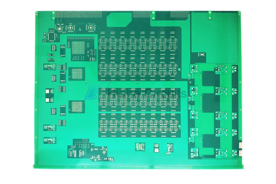
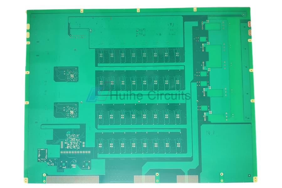
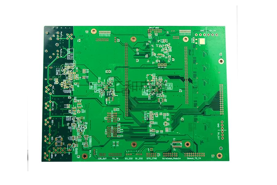
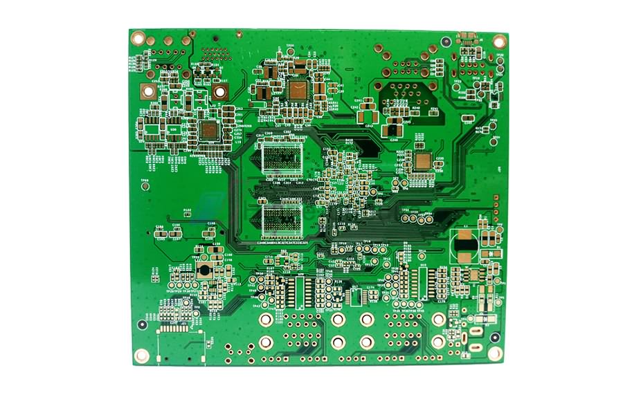
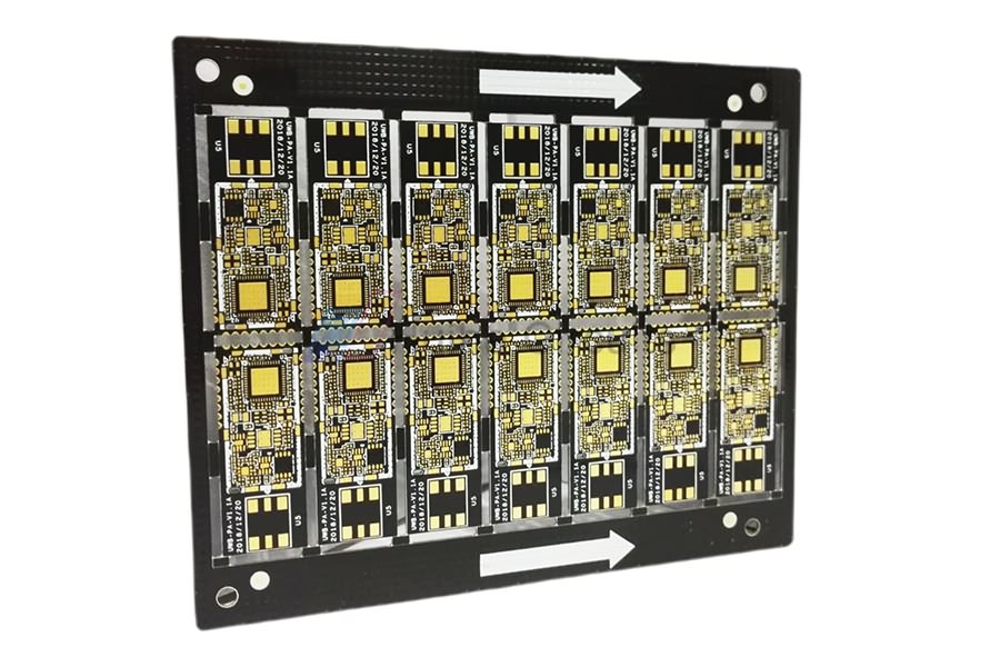
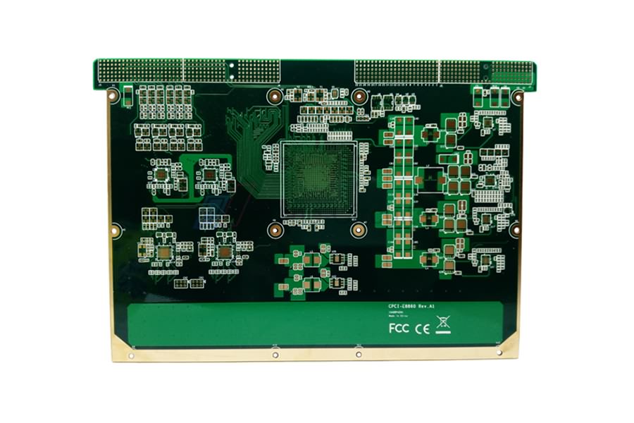
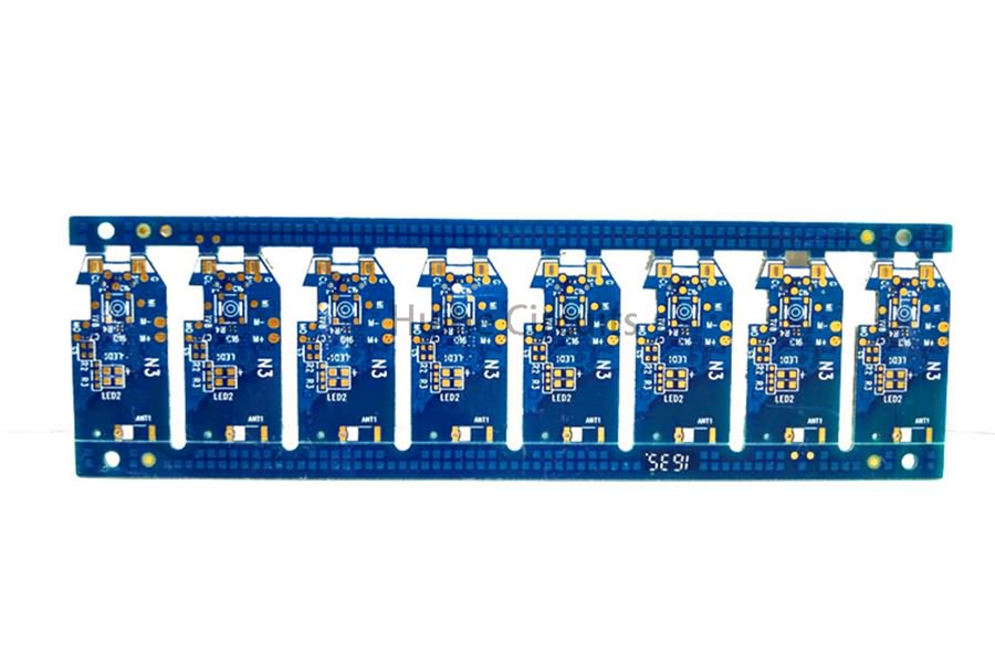
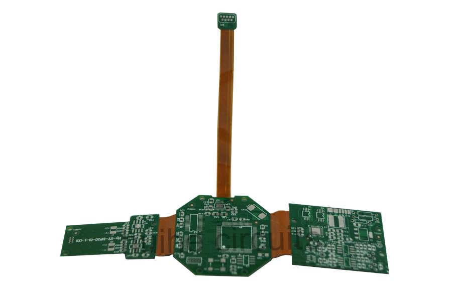
Product detail pictures:
Related Product Guide:
"Based on domestic market and expand abroad business" is our progress strategy for China Wholesale Flexible Pcb Fabrication Suppliers - 16 Layer ENIG Press Fit Hole PCB 31525 – Huihe , The product will supply to all over the world, such as: United Arab emirates, Hungary, Slovakia, They're durable modeling and promoting well all over the world. Under no circumstances disappearing key functions in a brief time, it's a should for you personally of fantastic quality. Guided by the principle of Prudence, Efficiency, Union and Innovation. the business make an awesome efforts to expand its international trade, raise its enterprise. rofit and improve its export scale. We are confident that we'll have a vibrant prospect and to be distributed all over the world in the years to come.
Sales manager is very enthusiastic and professional, gave us a great concessions and product quality is very good,thank you very much!
-
China Wholesale Flexible Pcb Factories - 6 Lay...
-
China Wholesale Order Printed Circuit Board Sup...
-
China Wholesale High Speed Pcb Suppliers - 6 L...
-
China Wholesale Rigid Flex Circuit Boards Quote...
-
China Wholesale Pcb Pwb Manufacturers - 8 laye...
-
China Wholesale Automatic Stabilizer Circuit Bo...


