
China Wholesale Emc Pcb Suppliers - 6 Layer ENIG Impedance Control PCB 14706 – Huihe
China Wholesale Emc Pcb Suppliers - 6 Layer ENIG Impedance Control PCB 14706 – Huihe Detail:
Difference between pad and via
1. Definitions differ
Pad: is the basic unit of surface mount assembly, which is used to form the landpattern of the circuit board, that is, a variety of combinations of pads designed for special component types.
Through hole: through hole is also called metallization hole. In the double panel and multilayer PCB, a common hole is drilled at the junction of the wires that need to be connected between the layers in order to connect the printed wires between layers. The main parameters of the hole are the outer diameter of the hole and the size of the hole.
The hole itself has parasitic capacitance and inductance to the ground, which often brings great negative effect to the circuit design.
2. Different principles
Pad: When a pad structure is not designed correctly, it is difficult to reach the desired weld point. Can be used for surface-mounted components or for plug-in components.
Through hole: In a circuit board, a line jumps from one side of the board to the other. The hole connecting the two wires is also called a hole (as opposed to a pad, there is no solder layer on the side). Also known as metallization hole, in the double panel and multilayer PCB, for connecting the printed wire between the layers, in each layer need to be connected at the intersection of the wire drilling on a public hole, that is, through the hole.
Technically, a layer of metal is PCB on the cylindrical surface of the hole wall of the hole through the chemical deposition method to connect the copper foil that needs to be connected in the middle layer, and the upper and lower sides of the hole through the shape of a circular solder pad, the parameters of the hole mainly include the outer diameter of the hole and the size of the hole.
3. Different effects
Through hole: the hole on PCB, play the role of conduction or heat dissipation.
Pad: it is the copper plate of PCB, some cooperate with the hole to connect, and some square plate, mainly used to paste parts.
Equipment display

Automatic Plating Line

PTH line

LDI

CCD Exposure Machine
Application

Communications

Security electronics

Railtransit
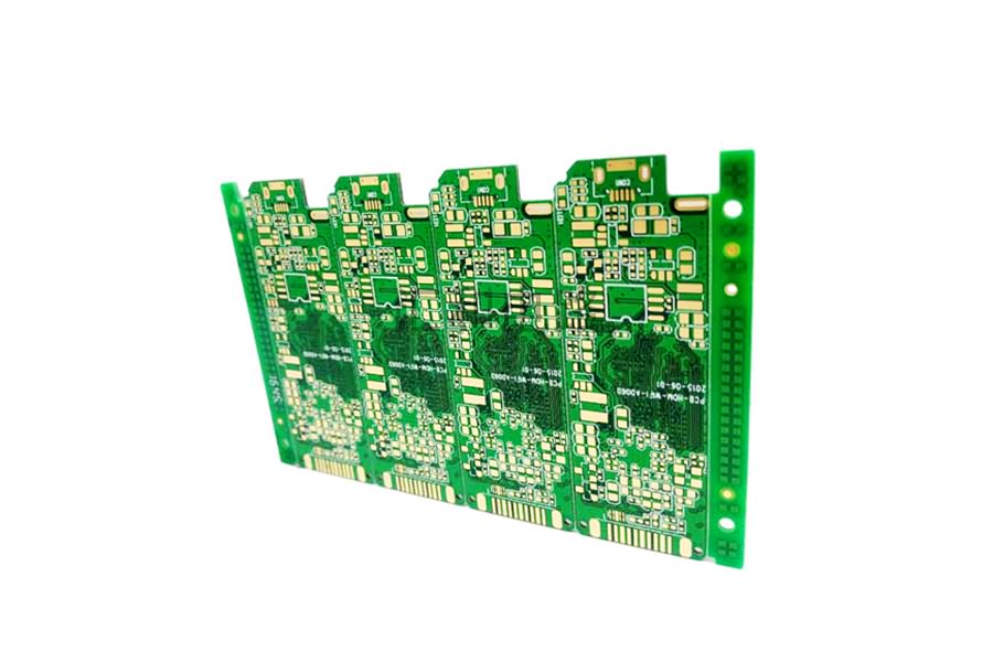
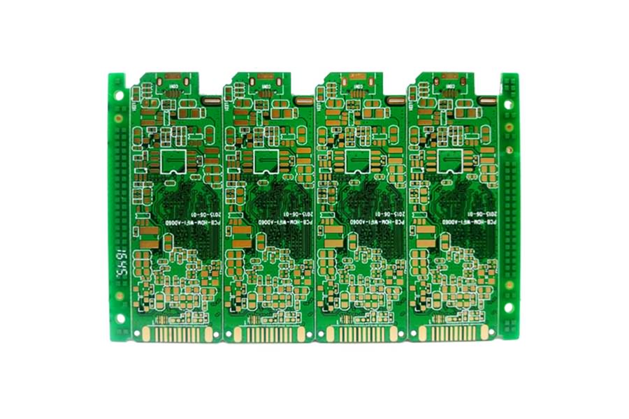
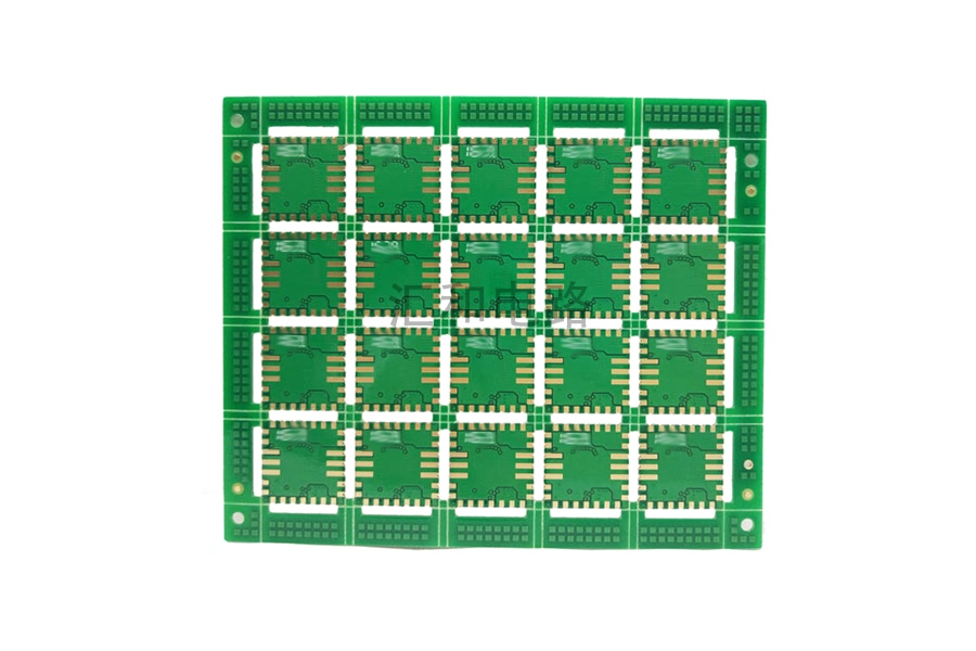
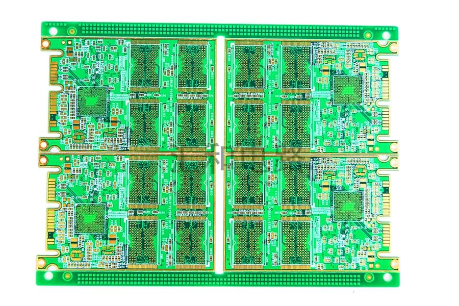
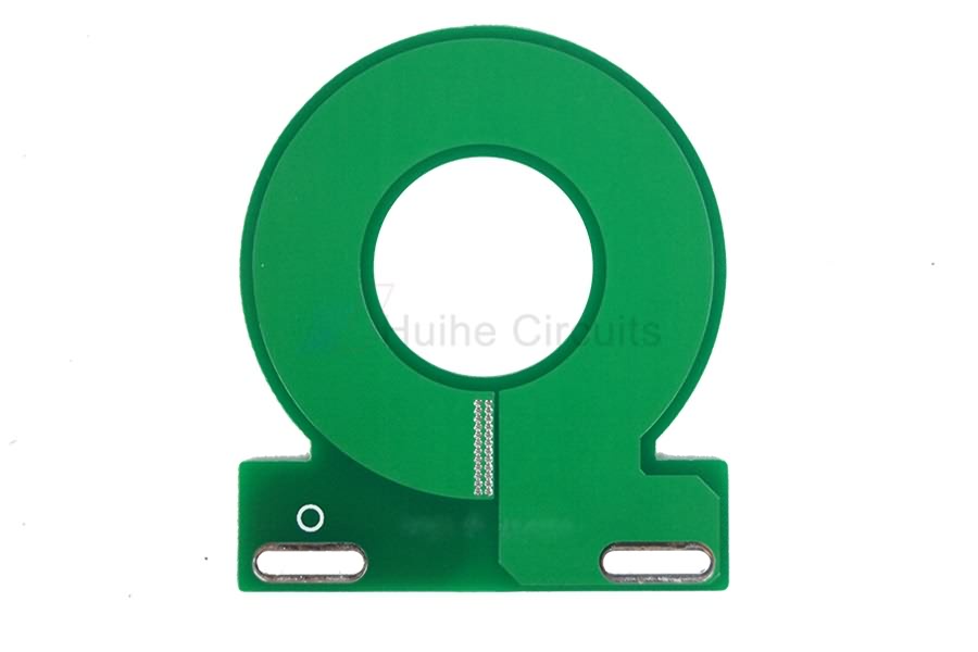
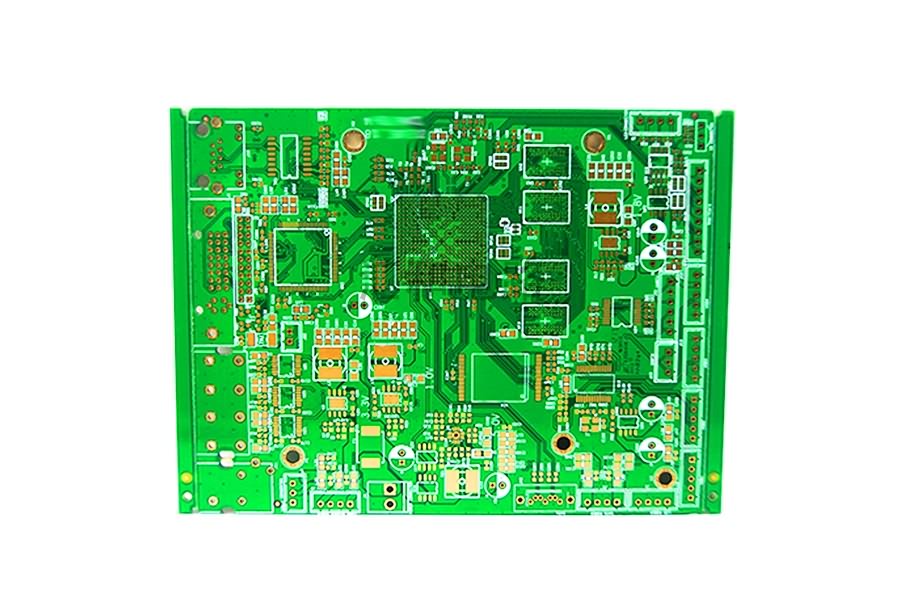
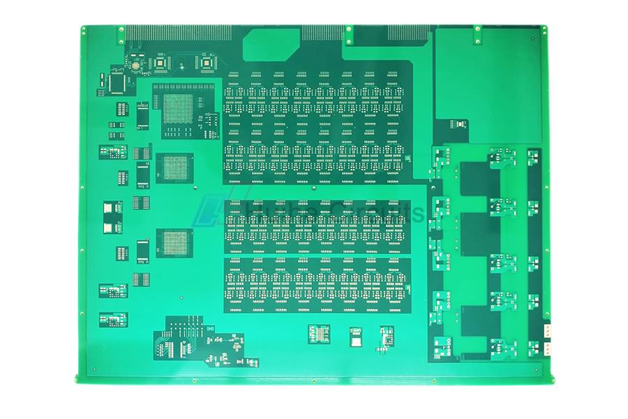
Product detail pictures:


Related Product Guide:
We depend on sturdy technical force and continually create sophisticated technologies to meet the demand of China Wholesale Emc Pcb Suppliers - 6 Layer ENIG Impedance Control PCB 14706 – Huihe , The product will supply to all over the world, such as: Netherlands, Macedonia, Ukraine, If you need to have any of our merchandise, or have other items to be produced, make sure you send us your inquiries, samples or in depth drawings. Meanwhile, aiming to develop into an international enterprise group, we look forward to receiving offers for joint ventures and other cooperative projects.
We have been engaged in this industry for many years, we appreciate the work attitude and production capacity of the company, this is a reputable and professional manufacturer.
-
China Wholesale Mp5 Circuit Board Suppliers - ...
-
China Wholesale Nixie Clock Pcb Factories - 8 ...
-
China Wholesale Circular Circuit Board Quotes -...
-

China Wholesale Pcb Board Power Supply Manufact...
-
China Wholesale Lcsc Pcb Quotes - 6 Layer High...
-
China Wholesale Flexible Pcb Prototype Quotes -...


