
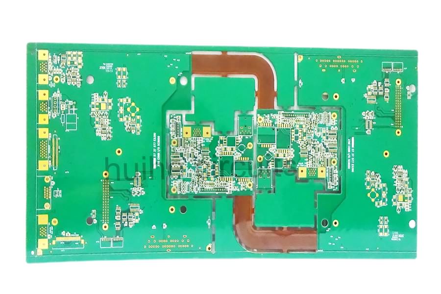
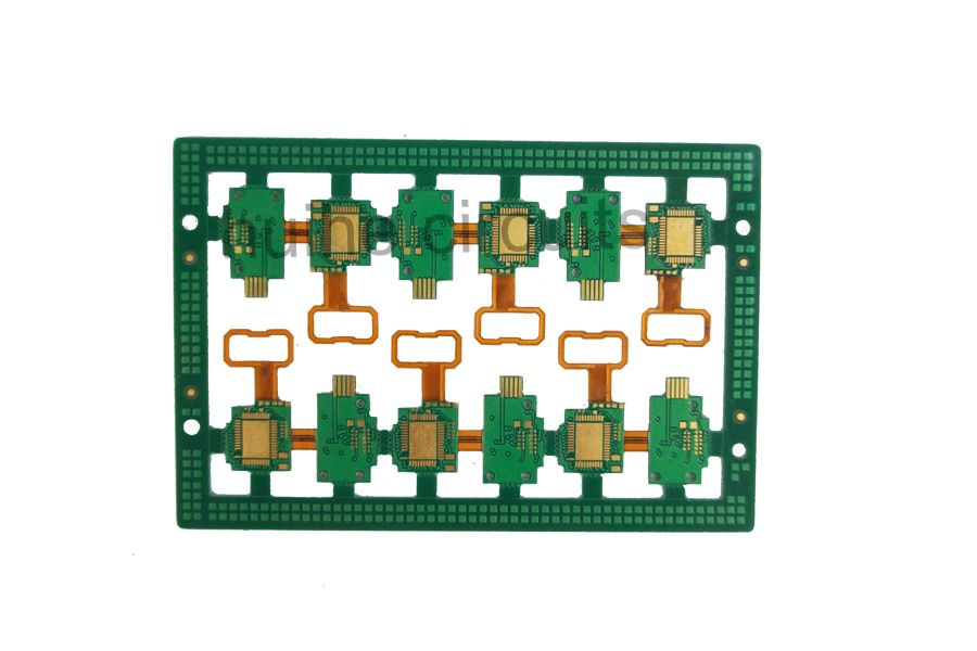
China Wholesale Double Sided Pcb Pricelist - 4 Layer ENIG Impedance Control Heavy Copper PCB – Huihe
China Wholesale Double Sided Pcb Pricelist - 4 Layer ENIG Impedance Control Heavy Copper PCB – Huihe Detail:
Precautions For Engineering Design Of Heavy Copper PCB
With the development of electronic technology, the volume of PCB is more and more small, density is becoming more and more high, and the PCB layers increasing, therefore, requires PCB on integral layout, anti-interference ability, process and manufacturability demand is higher and higher, as the content of engineering design very much, mainly for heavy copper PCB manufacturability, craft workability and the reliability of the product engineering design, it need to be familiar with the design standard and meet the requirements of production process, make the designed product smoothly.
1. Improve the uniformity and symmetry of inner layer copper laying
(1) Due to the superposition effect of inner layer solder pad and the limitation of resin flow, the heavy copper PCB will be thicker in the area with high residual copper rate than in the area with low residual copper rate after lamination, resulting in uneven thickness of the plate and affecting the subsequent patch and assembly.
(2) Because the heavy copper PCB is thick, the CTE of copper differs greatly from that of the substrate, and the deformation difference is large after pressure and heat. The inner layer of copper distribution is not symmetrical, and the warpage of the product is easy to occur.
The above problems need to be improved in the design of the product, in the premise of not affecting the function and performance of the product, the inner layer of the copper-free area as far as possible. The design of copper point and copper block, or changing the large copper surface to copper point laying, optimize the routing, make its density uniform, good consistency, make the overall layout of the board symmetrical and beautiful.
2. Improve the copper residue rate of inner layer
With the increase of copper thickness, the gap of the line is deeper. In the case of the same copper residual rate, the amount of resin filling needs to increase, so it is necessary to use multiple semi-cured sheets to meet the glue filling. When the resin is less, it is easy to lead to the lack of glue lamination and the uniformity of the thickness of the plate.
The low residual copper rate requires a large amount of resin to fill, and the resin mobility is limited. Under the action of pressure, the thickness of the dielectric layer between the copper sheet area, the line area and the substrate area has a great difference (the thickness of the dielectric layer between the lines is the thinnest), which is easy to lead to the failure of HI-POT.
Therefore, the copper residual rate should be improved as much as possible in the design of heavy copper PCB engineering, so as to reduce the need for glue filling, reduce the reliability risk of glue filling dissatisfaction and thin medium layer. For example, copper points and copper block design are laid in copper free area.
3. Increase line width and line spacing
For heavy copper PCBs, increasing the line width spacing not only helps to reduce the difficulty of etching processing, but also has a great improvement in laminated glue filling. The glass fiber cloth filling with small spacing is less, and the glass fiber cloth filling with large spacing is more. The large spacing can reduce the pressure of pure glue filling.
4. Optimize the inner layer pad design
For heavy copper PCB, because the copper thickness is thick, plus the superposition of the layers, copper has been in a large thickness, when drilling, the friction of the drill tool in the board for a long time is easy to produce the drill wear, and then affect the quality of the hole wall, and further affect the reliability of the product. Therefore, in the design stage, the inner layer of non-functional pads should be designed as few as possible, and no more than 4 layers are recommended.
If the design permits, the inner layer pads should be designed as large as possible. Small pads will cause greater stress in the drilling process, and the heat conduction speed is fast in the processing process, which is easy to lead to copper Angle cracks in the pads. Increase the distance between the inner layer independent pad and the hole wall as much as the design permits. This can increase the effective safe spacing between the hole copper and the inner layer pad, and reduce the problems caused by the hole wall quality, such as micro-short, CAF failure and so on
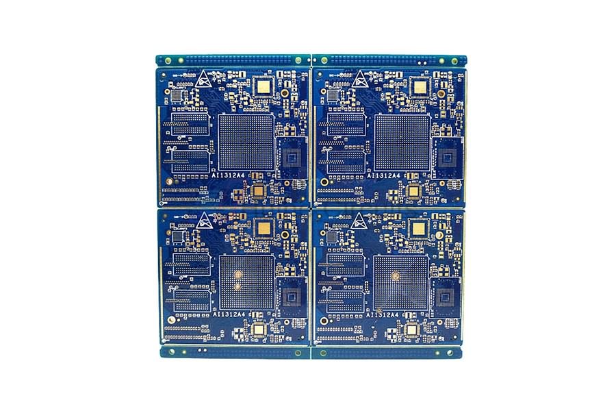
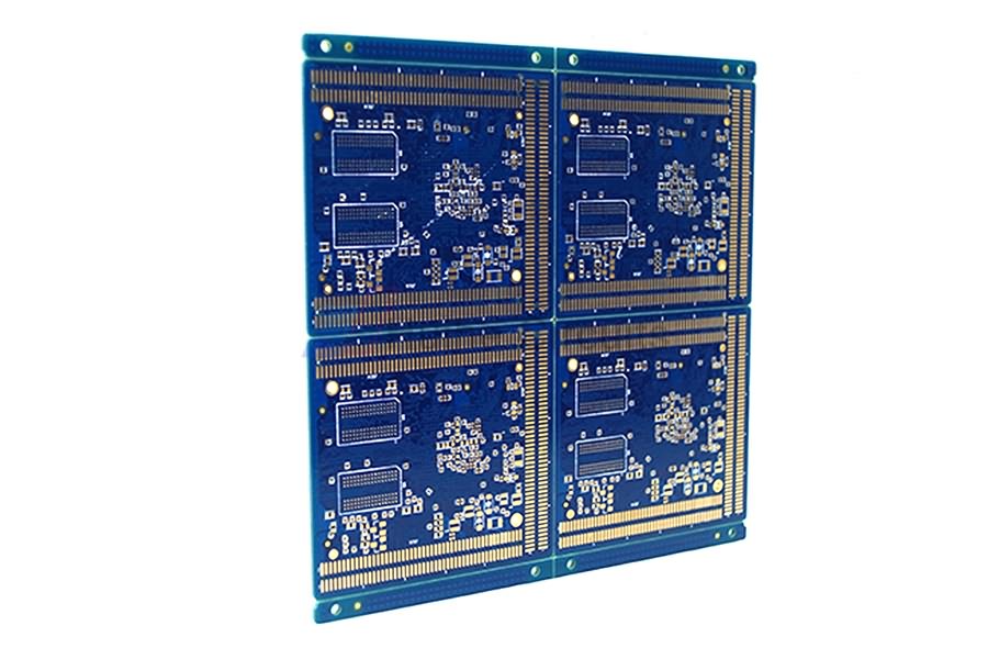
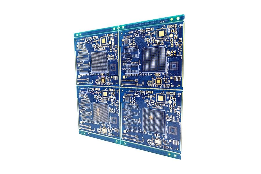
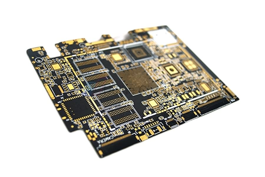
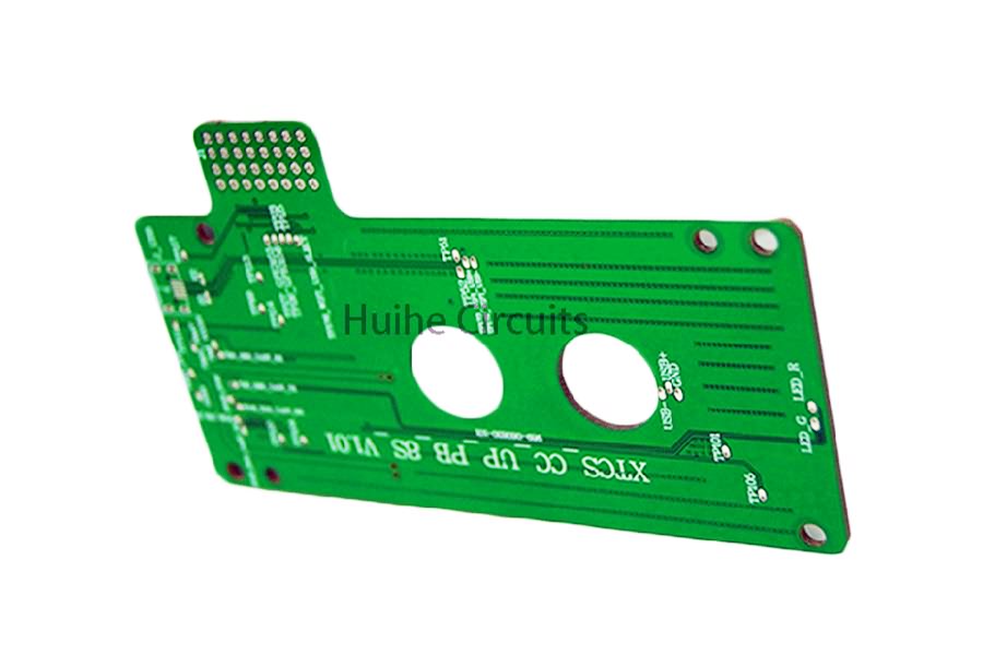
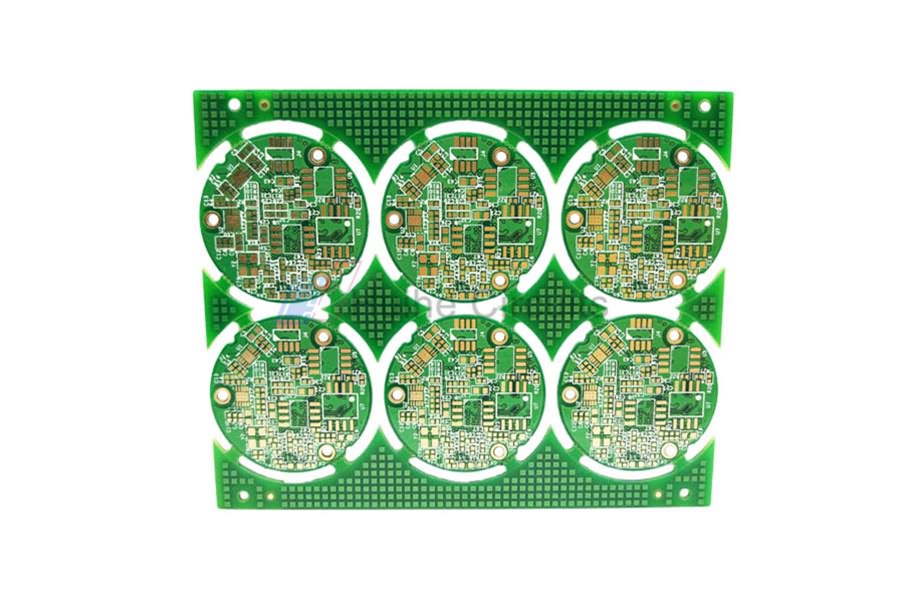
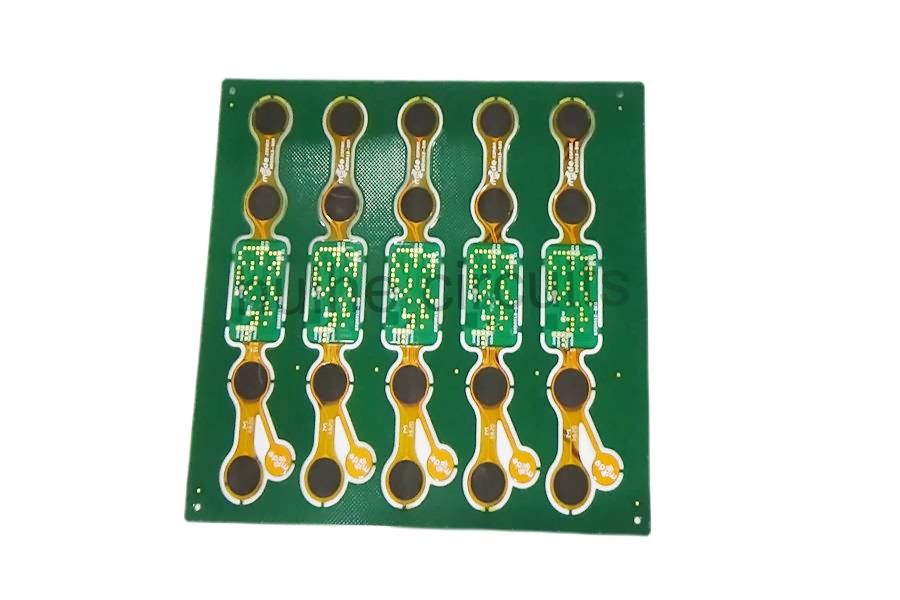
Product detail pictures:

Related Product Guide:
We always think and practice corresponding to the change of circumstance, and grow up. We aim at the achievement of a richer mind and body and the living for China Wholesale Double Sided Pcb Pricelist - 4 Layer ENIG Impedance Control Heavy Copper PCB – Huihe , The product will supply to all over the world, such as: Croatia, Zimbabwe, Rotterdam, In the increasingly competitive market, With sincere service high quality products and well-deserved reputation, we always offer customers support on products and techniques to achieve long-term cooperation. Living by quality, development by credit is our eternal pursuit, We firmly believe that after your visit we will become long-term partners.
The goods are very perfect and the company sales manager is warmful, we will come to this company to purchase next time.
-
China Wholesale Smt Boards Quotes - 6 layer E...
-
China Wholesale Timer Circuit Board Quotes - 8...
-
Personlized Products 6 Layers Pcb Manufacturer ...
-
China Wholesale Make Custom Pcb Pricelist - 8 ...
-
China Wholesale Pcb Power Board Factories - 4 ...
-
China Wholesale Populated Circuit Board Supplie...


