
China Wholesale Custom Pcb Suppliers - 10 Layer ENIG Blind Vias PCB 28526 – Huihe
China Wholesale Custom Pcb Suppliers - 10 Layer ENIG Blind Vias PCB 28526 – Huihe Detail:
About Blind Buried Via PCB
Blind Via: which enables the connection and conduction between the inner and outer layers
Buried Via: which can connect and guide between inner layers
Blind Vias are mostly small holes with a diameter of 0.05mm~0.15mm. There are laser hole forming, plasma etched hole and photoinduced hole forming, and laser hole forming is usually used.
HDI: High-density interconnection, non-mechanical drilling, micro-blind hole ring below 6mil, inside and outside layers of wiring line width/line gap is below 4mil, the diameter of the pad is not greater than 0.35mm is called HDI board production mode.
Blind Via
Blind Vias are used to connect one outer layer to at least one inner layer.
Each layer of blind hole needs to generate a separate drill file.
The ratio of hole depth to aperture (aspect ratio/thickness-diameter ratio) must be less than or equal to 1.
The keyhole determines the hole depth, that is, the maximum distance between the outermost layer and the inner layer.
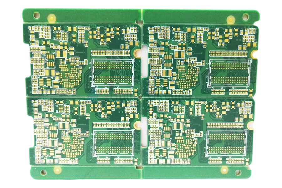
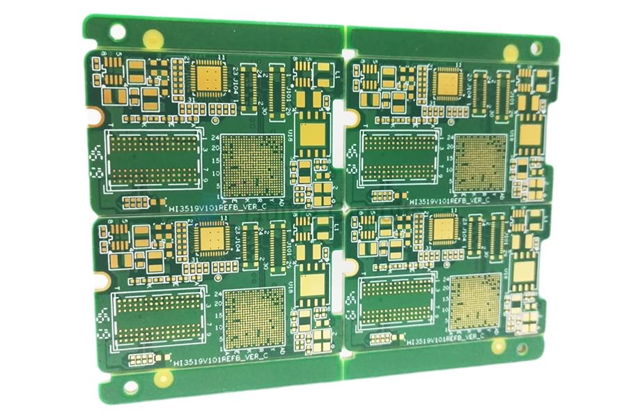
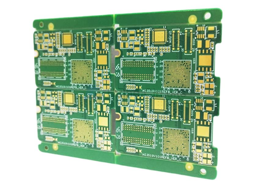
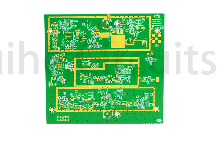
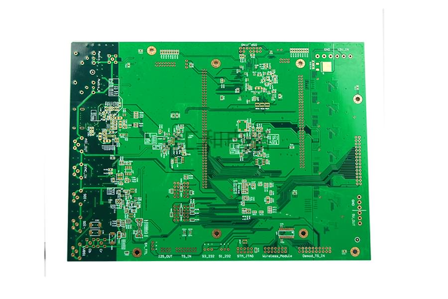
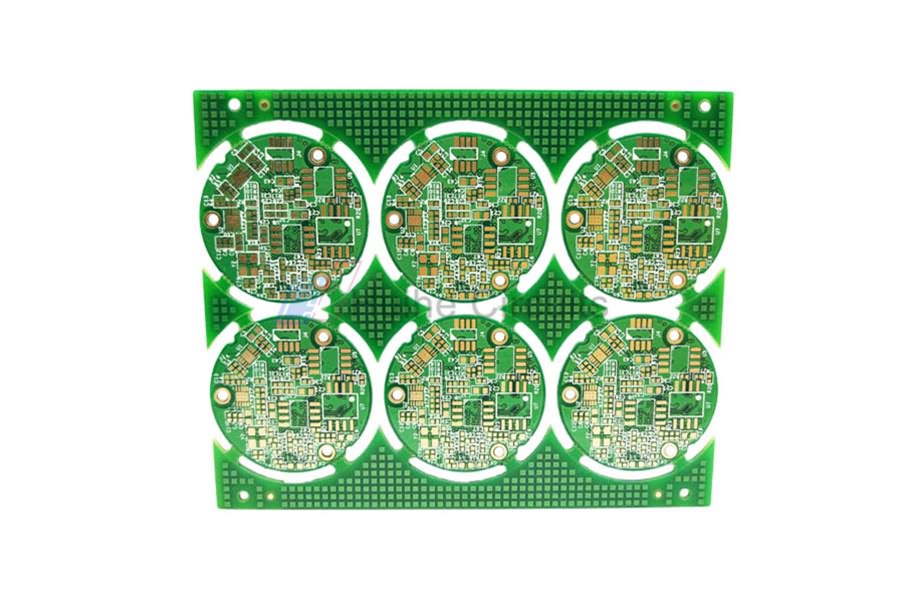
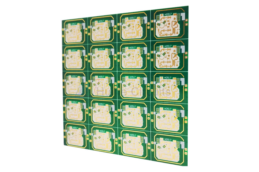
Product detail pictures:

Related Product Guide:
We rely upon strategic thinking, constant modernisation in all segments, technological advances and of course upon our employees that directly participate inside our success for China Wholesale Custom Pcb Suppliers - 10 Layer ENIG Blind Vias PCB 28526 – Huihe , The product will supply to all over the world, such as: Austria, Montpellier, Sri Lanka, We are proud to supply our products to every auto fan all around the world with our flexible, fast efficient services and strictest quality control standard which has always approved and praised by customers.
The company leader recept us warmly, through a meticulous and thorough discussion, we signed a purchase order. Hope to cooperate smoothly
-

China Wholesale Castellated Pcb Factories - 4 ...
-
China Wholesale Electric Circuit Board Manufact...
-
Manufacturer for Medical Pcb - 6 Layer ENIG RO...
-
China Wholesale Surface Mount Prototype Board F...
-
China Wholesale Electric Fence Circuit Board Qu...
-
China Wholesale Single Circuit Board Manufactur...


