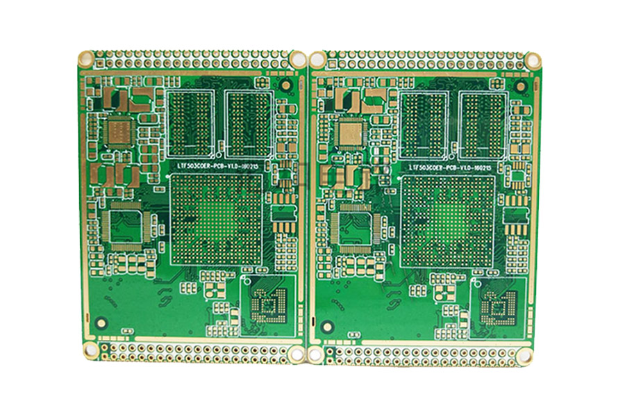
In the long – term design practice, people have summed up a lot of rules. If these principles can be followed in circuit design, it will be beneficial to the accurate debugging of the printed circuit board(PCB) control software and the normal operation of the hardware circuit. In summary, the principles to be followed are as follows:
(1) In terms of the layout of components, the components related to each other should be placed as close as possible. For example, clock generator, crystal oscillator, clock input end of CPU, etc., are prone to generate noise. When placed, they should be placed closer.
(2) Try to install decoupling capacitors next to key components such as ROM, RAM and other chips. The following points should be noted when placing decoupling capacitors:
1) The power input end of printed circuit board(PCB) is bonded to an electrolytic capacitor of about 100uF. If the volume allows, a larger capacity would be better.
2) In principle, a 0.1uF ceramic chip capacitor should be placed beside each IC chip. If the gap of the printed circuit board(PCB) is too small to be placed, 1-10uF tantalum capacitor can be placed around every 10 chips.
3) For components with weak anti-interference ability and storage components such as RAM and ROM with large current variation when turning off, decoupling capacitors should be connected between power line (VCC) and ground wire (GND).
4) The capacitor lead should not be too long. In particular, high frequency printed circuit board(PCB) bypass capacitors should not carry leads.
(3) Connectors are generally placed on the edge of the circuit board to facilitate installation and wiring work behind. If there is no way, it can be placed in the middle of the board, but try to avoid doing so.
(4) In the manual layout of components, the convenience of wiring should be considered as far as possible. For the areas with more wiring, enough space should be set aside to avoid wiring obstruction.
(5) Digital circuit and analog circuit should be arranged in different regions. If possible, a space of 2-3mm between them should be appropriate to avoid mutual interference.
(6) For circuits under high and low pressure, a space of more than 4mm should be set aside between them in order to ensure high enough electrical insulation reliability.
(7) The layout of components should be as neat and beautiful as possible.
Post time: Nov-16-2020


