
What is the role of PCB fabrication panel?
PCB panel
Printed circuit boards are widely used in various fields such as communications, aviation, automobiles, military, electric power, medical care, industrial control, electromechanical, and computers. What is PCB fabrication? Reproduction of products is called fabrication. Customers provide PCB fabrication documents and production requirements, and PCB manufacturers manufacture products according to requirements and charge processing fees. PCB fabrication means that PCB manufacturers reproduce printed circuit boards according to customer requirements.
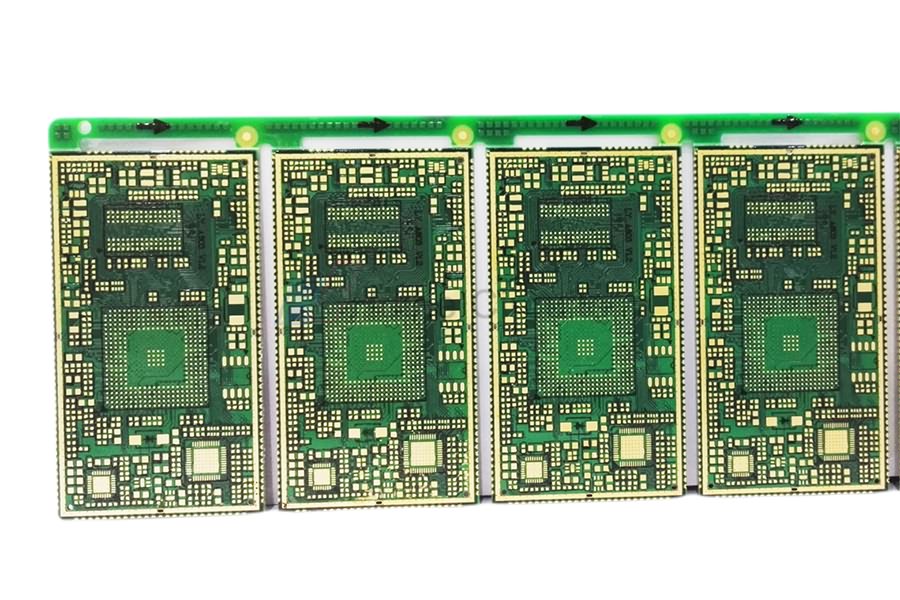
Why does PCB fabrication need to do panel work? After laying the SMT patch, does it need to be cut into a single board? What is the edge of the printed circuit board used for? Isn’t it said that the less the board is used, the cheaper it is? Usually most of the PCB fabrication will be PCB panel, and the early stage is to increase the production efficiency of the SMT patch production line. PCB splicing is only for the convenience of production. For PCB manufacturers, the base material of printed circuit boards is generally relatively large. Many boards are made at one time, and then cut one by one. The splicing is mainly used in welding production.
PCB panel has several functions, which are convenient for customers to plug in, convenient for PCB fabrication manufacturers to produce by themselves, and saves materials. PCB fabrication usually has several boards, such as two-in-one, four-in-one, etc. If you have the opportunity to go to the SMT patch production line, you will find that the difficulty of the SMT patch production line is actually in the tin high printing process, because even if the size of the printed circuit board is large, the printing time is almost 25s. That is to say, if the chip printing machine takes less time than the solder paste printing machine, it will wait empty. From the perspective of economic benefits, this is a waste.
PCB panel has another advantage. It can save time when picking and placing PCBA circuit boards, because multiple boards can be picked and placed at the same time. Man-hours wasted in picking and placing tools.
What is the purpose of PCB edge making? The main purpose of PCB edge design is to assist PCBA assembly production. The current SMT patch production line is actually very highly automated, and the boards are transported by belts and chains. The main purpose of the board edge is to transport the boards to these belts and chains. You can also leave a certain space around the board and don’t put any electronic parts. PCB fabrication generally requires at least 5.0mm or more, because the iron chain of the reflow furnace needs to use a relatively deep position on the edge of the board, so there is a chance to There is no need to design the edge of the board, otherwise the belt and chain may damage the electronic parts around it.
Post time: Nov-18-2022


