
Through-hole design in high speed PCB
In high speed PCB design, the seemingly simple hole often brings great negative effect to the circuit design. Through-hole (VIA) is one of the most important components of multilayer PCB boards, and the cost of drilling usually accounts for 30% to 40% of the PCB board cost. Simply put, every hole in a PCB can be called a through-hole.
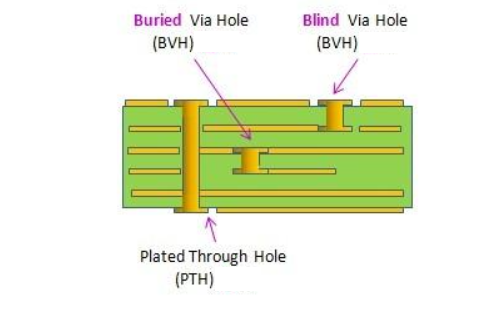
From the point of view of function, holes can be divided into two types: one is used for electrical connection between layers, the other is used for device fixation or positioning. In terms of technological process, these holes are generally divided into three categories, namely blind via, cand through via.
In order to reduce the adverse impact caused by the parasitic effect of the pore, the following aspects can be done as far as possible in the design:
Considering the cost and signal quality, a reasonable size hole is chosen. For example, for 6-10 layer memory module PCB design, it is better to choose a 10/20mil (hole/pad) hole. For some high-density small size board, you can also try to use 8/18mil hole. With the current technology, it is difficult to use smaller perforations. For the power supply or ground wire hole can be considered to use a larger size, to reduce the impedance.
From the two formulas discussed above, it can be concluded that the use of a thinner PCB board is beneficial to reducing the two parasitic parameters of the pore.
The pins of the power supply and ground should be drilled nearby. The shorter the leads between the pins and the holes, the better, as they will lead to an increase in inductance. At the same time, the power supply and ground leads should be as thick as possible to reduce impedance.
The signal wiring on the high-speed PCB board should not change layers as much as possible, that is, to minimize unnecessary holes.
Some grounded holes are placed near the holes in the signal exchange layer to provide a close loop for the signal. You can even put a lot of extra ground holes on the PCB board. Of course, you need to be flexible in your design. The through-hole model discussed above has pads in each layer. Sometimes, we can reduce or even remove pads in some layers.
Especially in the case of very large pore density, it may lead to the formation of a broken groove in the copper layering of the partition circuit. To solve this problem, in addition to moving the position of the pore, we can also consider reducing the size of the solder pad in the copper layering.
How to use over holes: Through the above analysis of the parasitic characteristics of over holes, we can see that in high-speed PCB design, the seemingly simple improper use of over holes will often bring great negative effects to the circuit design.
Post time: Aug-19-2022


