-
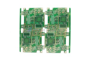
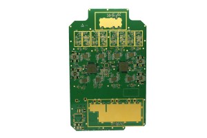
8 Layer ENIG FR4 Via-In-Pad PCB
Layers: 8
Surface finish: ENIG
Base material: FR4
Outer Layer W/S: 4.5/3.5mil
Inner layer W/S: 4.5/3.5mil
Thickness: 1.2mm
Min. hole diameter:0.15mm
Special process: via-in-pad
-
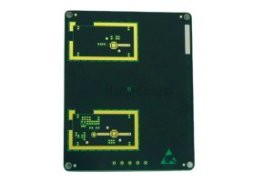
6 Layer FR4 ENIG Via In Pad PCB
Layers: 6
Surface finish: ENIG
Base material: FR4
Outer Layer W/S: 4/3.5mil
Inner layer W/S: 4.5/3.5mil
Thickness: 1.0mm
Min. hole diameter:0.2mm
Special process: via in pad
-
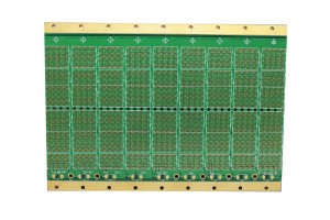
10 Layer Impedance Control Resin Plugging PCB
Layers: 10
Surface finish: ENIG
Aspect Ratio: 8:1
Base material: FR4
Outer Layer W/S: 4/4mil
Inner layer W/S: 5/3.5mil
Thickness: 2.0mm
Min. hole diameter:0.25mm
Special process: Impedance Control, Resin Plugging, Different Copper Thickness
-
10 Layer ENIG FR4 Impedance Control PCB
Layers: 10
Surface finish: ENIG
Base material: FR4
Outer Layer W/S: 4/4mil
Inner layer W/S: 5/3.5mil
Thickness: 2.0mm
Min. hole diameter: 0.25mm
Thickness diameter ratio:8:1
-
8 Layer ENIG FR4 Via-In-Pad PCB
Layers: 8
Surface finish: ENIG
Base material: FR4
Outer Layer W/S: 4/3.5mil
Inner layer W/S: 4/3.5mil
Thickness: 1.0mm
Min. hole diameter:0.2mm
Special process: via-in-pad, impedance control
-
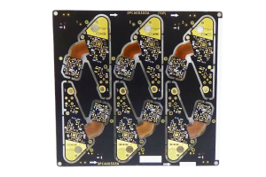
4 Layer ENIG RO4003+AD255 Mixed Lamination PCB
Layers: 4
Surface finish: ENIG
Base material: Arlon AD255+Rogers RO4003C
Min. hole diameter: 0.5mm
Minimum W/S:7/6mil
Thickness: 1.8mm
Special process:Blind hole -
12 Layer FR4 ENIG Impedance Control PCB
Layers: 12
Surface finish: ENIG
Base material: FR4
Outer Layer W/S: 5/4mil
Inner layer W/S: 4/5mil
Thickness: 3.0mm
Min. hole diameter: 0.3mm
Special process: 5/5mil impedance control line -
6 Layer ENIG Automotive Radar Rigid Flex PCB
Layer: 6
W/S: 4/4mil
Board Thickness: 1.6mm
MIn. Hole Diameter: 0.2mm
Special Processing:level 1 HDI
Blind Via:0.07mm
Surface Finish: ENIG
laminate:2R+2F+2R
Application Industry: automotive radar -
8 Layer ENIG FR4 Multilayer PCB
Layers: 8
Surface finish: ENIG
Base material: FR4
Outer Layer W/S: 4/4mil
Inner layer W/S: 3.5/3.5mil
Thickness: 1.6mm
Min. hole diameter: 0.45mm -
4 Layer ENIG FR4 Blind Buried Vias PCB
Layers: 4
Surface finish: ENIG
Base material: FR4 Tg170
Outer Layer W/S: 5.5/6mil
Inner layer W/S: 17.5mil
Thickness: 1.0mm
Min. hole diameter: 0.5mm
Special process: Blind Vias -
10 Layer ENIG FR4 Via In Pad PCB
Layer: 10
Surface finish: ENIG
Material: FR4 Tg170
Outer line W/S: 10/7.5mil
Inner line W/S: 3.5/7mil
Board thickness: 2.0mm
Min. hole diameter: 0.15mm
Plug hole: via filling plating -
4 Layer ENIG FR4 Half Hole PCB
Layers: 4
Surface finish: ENIG
Base material: FR4
Outer Layer W/S: 9/4mil
Inner layer W/S: 7/4mil
Thickness: 0.8mm
Min. hole diameter: 0.2mm
Special process:Impedance, half hole


