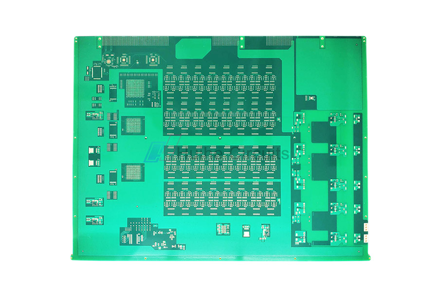
Development History of PCB Board
Since the birth of PCB board, it has developed for more than 70 years. In the development process of more than 70 years, PCB has undergone some important changes, which has promoted the rapid development of PCB and made it rapidly applied to various fields. Throughout the development history of PCB, it can be divided into six periods.
(1) The birth date of PCB. PCB was born from 1936 to the late 1940s. In 1903, Albert Hanson first used the concept of “line” and applied it to the telephone switching system. The design idea of this concept is to cut thin metal foil into circuit conductors, then glue them to paraffin paper, and finally paste a layer of paraffin paper on them, thus forming the structural prototype of today’s PCB. In 1936, Dr. Paul Eisner really invented the manufacturing technology of PCB. This time is usually regarded as the real birth time of PCB. In this historical period, the manufacturing processes adopted for PCB are coating method, spray method, vacuum deposition method, evaporation method, chemical deposition method and coating method. At that time, PCB was typically used in radio receivers.
(2) Trial production period of PCB. The PCB trial production period was in the 1950s. With the development of PCB, since 1953, the communication equipment manufacturing industry began to pay more attention to PCB and began to use PCB in large quantities. In this historical period, the manufacturing process of PCB is the subtraction method. The specific method is to use copper-clad thin paper-based phenolic resin laminate (PP material), and then use chemicals to dissolve the unwanted copper foil, so that the remaining copper foil forms a circuit. At this time, the chemical composition of the corrosive solution used for PCB is ferric chloride. The representative product is the portable transistor radio manufactured by Sony, which is a single-layer PCB with PP substrate.
(3) Useful life of PCB. PCB was put into use in the 1960s. Since 1960, Japanese companies began to use GE base materials (copper-clad glass cloth epoxy resin laminate) in large quantities. In 1964, the American optical circuit company developed the electroless copper plating solution (cc-4 solution) for heavy copper, thus starting a new addition method manufacturing process. Hitachi introduced cc-4 technology to solve the problems of heating warping deformation and copper stripping of domestic Ge substrates at the initial stage. With the initial improvement of material technology, the quality of Ge base materials continues to improve. Since 1965, some manufacturers began to mass produce Ge substrates, Ge substrates for industrial electronic equipment and PP substrates for civil electronic equipment in Japan.
Post time: Jun-28-2022


