
Via Process in Multilayer PCB Fabrication
Vias are one of the important components of multilayer PCB fabrication, and the cost of drilling usually accounts for 30% to 40% of the cost of PCB prototype. The via hole is the hole drilled on the copper clad laminate. It carries the conduction between the layers and is used for electrical connection and fixing of devices. ring.
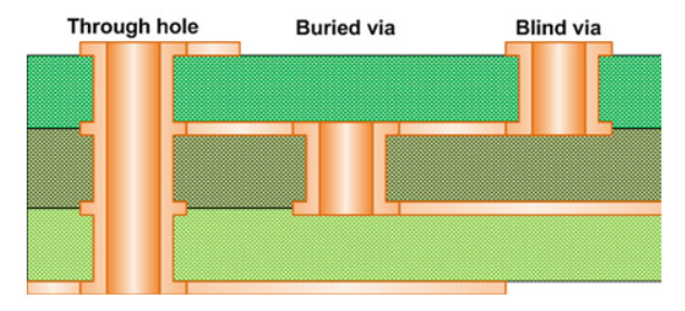
From the process of multilayer PCB fabrication, vias are divided into three categories, namely, holes, buried holes and through holes. In multilayer PCB fabrication and production, common via processes include via cover oil, via plug oil, via window opening, resin plug hole, electroplating hole filling, etc. Each process has its own characteristics.
1. Via cover oil
The “oil” of the via cover oil refers to the solder mask oil, and the via hole cover oil is to cover the hole ring of the via hole with solder mask ink. The purpose of the via cover oil is to insulate, so it is necessary to ensure that the ink cover of the hole ring is full and thick enough, so that tin will not stick to the patch and DIP later. It should be noted here that if the file is PADS or Protel, when it is sent to a multilayer PCB fabrication factory for via cover oil, you must carefully check whether the plug-in hole (PAD) uses via, and if thus, your plug-in hole will be covered with green oil and cannot be welded.
2. Via window
There is another way to deal with “via cover oil” when the via hole is opened. The via hole and the grommet should not be covered with solder mask oil. The opening of the via hole will increase the heat dissipation area, which is conducive to heat dissipation. Therefore, if the heat dissipation requirements of the board are relatively high, the opening of the via hole can be selected. In addition, if you need to use a multimeter to do some measurement work on the vias during multilayer PCB fabrication, then make the vias open. However, there is a risk of opening the via hole – it is easy to cause the pad to be shortened to the tin.
3. Via plug oil
Via plugging oil, that is, when the multilayer PCB is processed and produced, the solder mask ink is first plugged into the via hole with an aluminum sheet, and then the solder mask oil is printed on the whole board, and all the via holes will not transmit light. The purpose is to block the vias to prevent tin beads from hiding in the holes, because the tin beads will flow to the pads when they are dissolved at high temperature, causing short circuits, especially on BGA. If the vias do not have proper ink, the edges of the holes will turn red, cause “false copper exposure” is bad. In addition, if the via hole plugging oil is not done well, it will also affect the appearance.
4. Resin plug hole
The resin plug hole simply means that after the hole wall is plated with copper, the via hole is filled with epoxy resin, and then copper is plated on the surface. The premise of the resin plug hole is that there must be copper plating in the hole. This is because the use of resin plug holes in PCBs is often used for BGA parts. Traditional BGA may use via between the PAD and the PAD to route the wires to the back. However, if the BGA is too dense and the Via cannot go out, it can be drilled directly from the PAD. Do Via to another floor to route cables. The surface of the multilayer PCB fabrication by the resin plug hole process has no dents, and the holes can be turned on without affecting the soldering. Therefore, it is favored on some products with high layers and thick boards.
5. Electroplating and hole filling
Electroplating and filling means that the vias are filled with electroplated copper during multilayer PCB fabrication, and the bottom of the hole is flat, which is not only conducive to the design of stacked holes and via in pads, but also helps to improve electrical performance, heat dissipation, and reliability.
Post time: Nov-12-2022


