
Development trend of printed circuit board(PCB)
Ever since the early 20th century, when telephone switches pushed circuit boards to become denser, the printed circuit board(PCB) industry has been searching for higher densities to meet the insatiable demand for smaller, faster and cheaper electronics. The trend toward increasing density has not abated at all, but has even accelerated. With the enhancement and acceleration of integrated circuit function every year, the semiconductor industry guides the development direction of PCB technology, promotes the circuit board market, and also speeds up the development trend of printed circuit board(PCB).
Since the increase in integrated circuit integration leads directly to the increase in input/output (I/O) ports (Rent’s law), the package also needs to increase the number of connections to accommodate the new chip. At the same time, package sizes are constantly being tried to get smaller. The success of planar array packaging technology has made it possible to produce more than 2000 leading-edge packages today, and this number will grow to nearly 100000 within a few years as super-Super computers evolve. IBM’s Blue Gene, for example, helps classify vast amounts of genetic DNA data.
The PCB must keep up with the density curve of the package and adapt to the latest compact package technology. Direct chip bonding, or flip chip technology, attaches chips directly to a circuit board: bypassing conventional packaging altogether. The enormous challenges that flip chip technology poses to circuit board companies have only been addressed in a small part and are limited to a small number of industrial applications.
PCB supplier has finally reached many of the limits of using traditional circuit processes and must continue to evolve, as once expected, with reduced etching processes and mechanical drilling being challenged. The flexible circuit industry, often neglected and neglected, has led the new process for at least a decade. Semi-additive conductor fabrication techniques can now produce copper printed lines less than the width of ImilGSfzm, and laser drilling can produce microholes of 2mil (50Mm) or less. Half of these numbers can be achieved in small process development lines, and we can see that these developments will be commercialized very quickly.
Some of these methods are also used in the rigid circuit board industry, but some of them are difficult to implement in this field because things like vacuum deposition are not commonly used in the rigid circuit board industry. The share of laser drilling can be expected to increase as packaging and electronics demand more HDI boards; The rigid circuit board industry will also increase the use of vacuum coating to make high density semi-addition conductor molding.
Finally, the multilayer PCB board process will continue to evolve and the market share of the multilayer process will increase. PCB manufacturer will also see epoxy polymer system circuit boards lose their market in favor of polymers that can be used better for laminates. The process could be accelerated if epoxy-containing flame retardants were banned. We also note that flexible boards have solved many of the problems of high density, they can be adapted to higher temperature lead-free alloy processes, and flexible insulation materials do not contain desert and other elements on the environmental “killer list.”
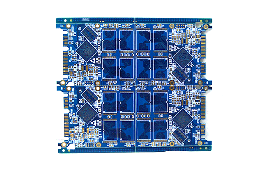
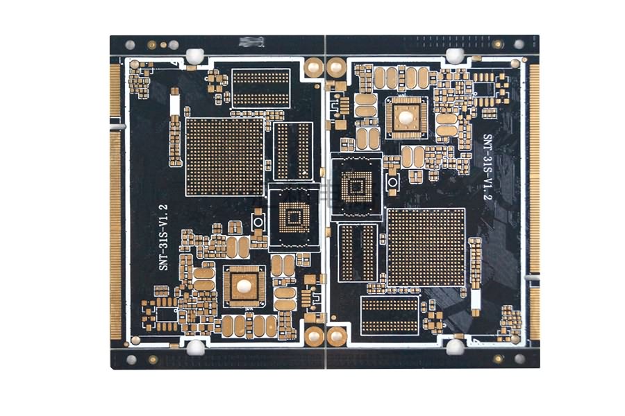
Huihe Circuits is a PCB manufacturing company, using lean production methods to ensure that each customer’s PCB product can be shipped on time or even ahead of schedule. Choose us, and you don’t have to worry about the delivery date.
Post time: Jul-26-2022


