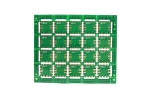
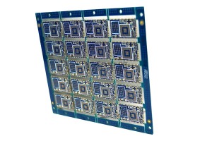
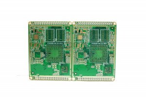
4 Layer ENIG Impedance Half Hole PCB
Processing Method Of Metallized Half Hole PCB Drilling
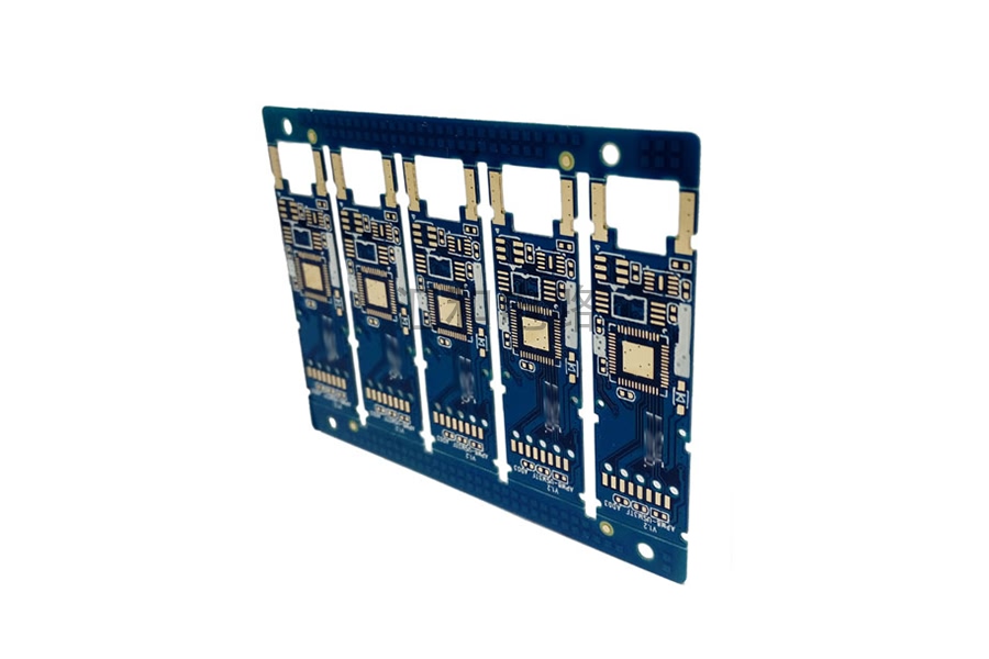
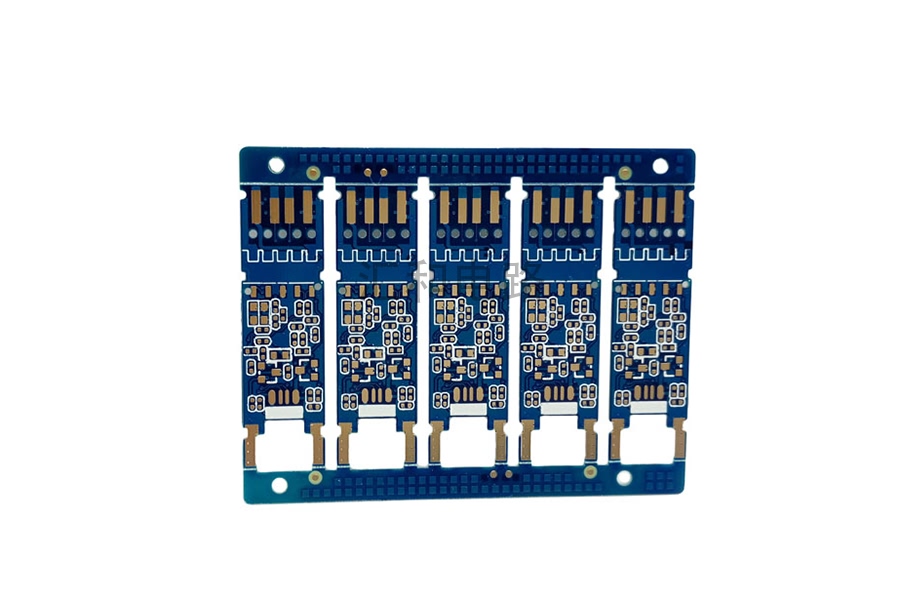
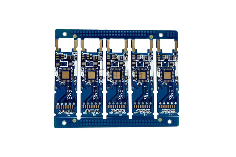
The specific metallized half-hole shall be processed in the following way: all metallized half-hole PCB holes shall be drilled in the way of drilling after drawing plating and before etching, one hole shall be drilled at the intersection points at both ends of the half-hole.
1) Formulate the MI process according to the technological process,
2) the metal half hole is a drill drill (or gong out), figure after plating, before etching two drill half hole, must consider the shape of the gong groove will not expose copper, drill half hole to the unit move,
3) Right hole (drill half hole)
A. Drill first, and then turn the plate over (or mirror direction); Drill hole on the left
B. The purpose is to reduce the pulling of the drill knife on the copper in the inner hole of the half hole, resulting in the loss of copper in the hole.
4) According to the spacing of the contour line, the size of the drill nozzle of the half hole is determined.
5) Draw resistance welding film, and the gongs are used as the blocking point to open the window and enlarge the window by 4mil
Equipment Display

PCB Automatic Plating Line

PCB PTH Line

PCB LDI

PCB CCD Exposure Machine
Factory Show

PCB Manufacturing Base

Admin Receptionist

Meeting Room