-
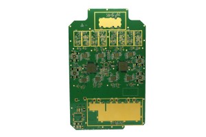
Good Quality High-Tg Circuit Boards - 8 Layer ENIG FR4 Multilayer PCB – Huihe
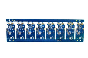
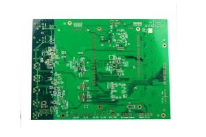
The Difficulty Of Multilayer PCB Board Prototyping 1. The difficulty of interlayer alignment Because of the many layers of multilayer PCB board, the calibration requirement of PCB layer is higher and higher. Typically, alignment tolerance between layers is controlled at 75um. It is more difficult to control the alignment of multilayer PCB board because of the large size of the unit, the high temperature and humidity in the graphics conversion workshop, the dislocation overlap caused by t... -
Hot Selling for Electronic Pcb Board - 8 Layer FPC+FR4 Rigid Flex PCB – Huihe
Rigid Flex PCB Plays A Key Role In The Automotive Market The Rigid Flex PCB is becoming more and more important in automotive electronics, which is beyond PCB operators’ original imagination. The reason is that we did not think that the technology used in mobile phone lens module would have the opportunity to extend to the ADAS lens module for car, and further attract the auto component industry to introduce the Rigid Flex PCB into the module products such as photar, and become the entry bric... -
Manufactur standard Quick Pcb Fabrication - 6 Layer FR4 ENIG Impedance Control PCB – Huihe
About The Impedance Impedance is the combination of capacitance and inductance to block the circuit in high frequency signal. Impedance is a kind of AC characteristic, which means that it is related to frequency and is used to describe the high frequency characteristics of PCB. Factors Affecting Impedance DK (R): determined by raw materials (PCB material, semi cured sheet) Line Thickness (T): determined by raw materials and process capability. Line Width (W): determined by customer’s original... -
OEM Supply Prototyping Board Factory - 6 Layer ENIG FR4 Heavy Copper PCB – Huihe
Crack problem of inner thick brazing pad The demand for heavy copper PCB is increasing, and the inner layer pads are getting smaller and smaller. The problem of pad cracking often occurs during PCB drilling (mainly for large holes above 2.5mm). There is little room for improvement in the material aspect of this kind of problem. The traditional improvement method is to increase the pad, increase the peeling strength of the material, and reduce the drilling rate, etc. Based on the analysis of P... -
China Factory for Rapid Pcb Prototype - 8 Layer HASL Multilayer FR4 PCB – Huihe
Why Are Multilayer PCB Boards Mostly Even? Due to the lack of a layer of medium and foil, the cost of raw materials for odd PCB is slightly lower than that for even PCB. However, the processing cost of odd layer PCB is significantly higher than that of even layer PCB. The processing cost of the inner layer is the same, but the foil/core structure significantly increases the processing cost of the outer layer. Odd layer PCB needs to add non-standard lamination core layer bonding process o... -
Chinese wholesale Circuit Board Fabrication - 6 Layer ENIG Impedance Half Hole PCB – Huihe
How To Identify A Half Hole In Your Design File ? Half hole PCB is designed because of the structure of the device and circuit board plug-in A single or whole rowof device holes are directly added to the outline of the metalized half hole to ensure that half of the deviceholes are in the board and half are out of the board . The Gerber file should contain the following: 01.Line layer(GTL and GBL) Half hole brazing pads are located at top and bottom 02.Weld barer layer(GTS and GBS... -
OEM manufacturer Sensor Circuit Board - 8 Layer ENIG FR4 Via-In-Pad PCB – Huihe
The most difficult thing to control the plug hole in the via-in-pad is the solder ball or pad on the ink in the hole. Due to the necessity of using high density BGA (ball grid array) and the miniaturization of SMD chip, the application of in tray hole technology is more and more. Through the reliable through hole filling process, the in plate hole technology can be applied to the design and manufacture of high-density multilayer board, and avoid abnormal welding. HUIHE Circuits has been using... -
High definition China Quick Turn Pcb Factory - 10 Layer ENIG FR4 Tg150 PCB – Huihe
Advantages Of High Tg PCB Materials The main advantage of high Tg materials is higher operating temperature (MOT), which can carry more current. According to experience, TG minus about 20 ℃ can be used as mot. At this temperature, the PCB can run normally for a long time without damage. The heat resistance temperature of the common solder mask is usually lower than the Tg of the substrate. The conventional maximum operating temperature of solder mask is about 150 ℃. For high Tg applicati... -

Manufactur standard Fpc Flexible Pcb Circuit Board - 6 Layer FR4 ENIG Impedance Control PCB – Huihe
Factors Determining Controlled Impedance The characteristic impedance of a PCB is usually determined by its inductance and capacitance, resistance and conductance. These factors are functions of the physical size of the circuit, the dielectric constant and dielectric thickness of the PCB substrate material. In general, the line impedance of a PCB ranges from 25 to 125Ω. The PCB structure that determines the impedance value consists of the following factors: Width and thickness of top and bott... -
Reliable Supplier Two Layer Pcb - 6 Layer FR4 ENIG Impedance Control PCB – Huihe
PCB Impedance Line Design 1.In the process of PCB LAYOUT, consider the basic conditions required to control the impedance are: line width, line distance, line length, impedance line shielding reference layer, according to these requirements will be placed in the appropriate position of the impedance line. 2. The shielding reference layer preferentially selects the line adjacent to the layer where the impedance line is located. The corresponding position of the impedance line is a complete cop... -
OEM manufacturer Prototype Pcb Assembly Manufacturer - 8 Layer ENIG FR4 Half Hole PCB – Huihe
Half Hole Technology After the PCB is made in the half hole, the tin layer is set at the edge of the hole by electroplating. The tin layer is used as the protective layer to enhance the tear resistance and completely prevent the copper layer falling off from the hole wall. Therefore, the impurity generation in the production process of the printed circuit board is reduced, and the workload of cleaning is also reduced, so as to improve the quality of the finished PCB. After the production of c... -
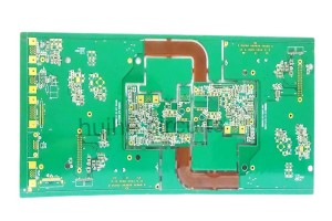
Super Purchasing for Quick Pcb Prototyping - 6 Layer ENIG FR4+RO4350 Mixed Lamination PCB – Huihe
Multilayer Mixed Lamination High Frequency PCB Multilayer mixed lamination PCB board needs to use materials with different characteristics than traditional multilayer PCB board. Mixing PCBs can be a mixture of FR4 and hf PCBs, or a mixture of HF PCBs from different DKs. With technological innovation, hybrid structures are becoming more and more popular. This brings benefits, but the challenges also need to be better understood. Advantages Of Mixing Lamination High Frequency PCB Impo...


