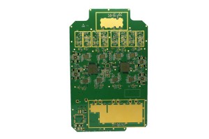
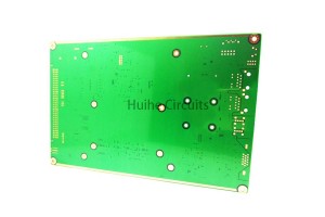
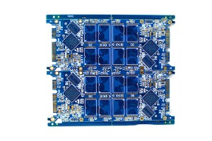
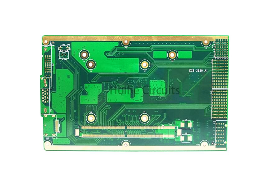
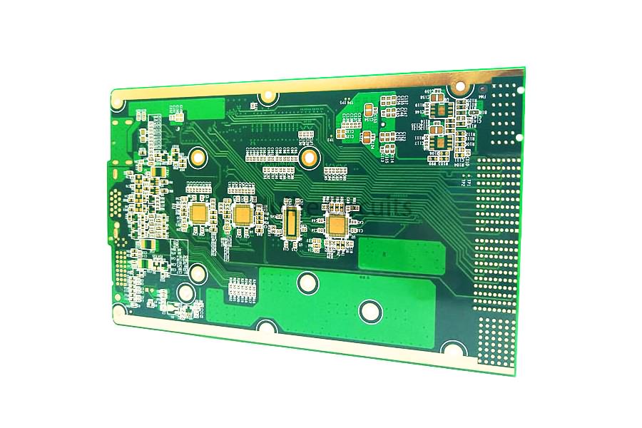
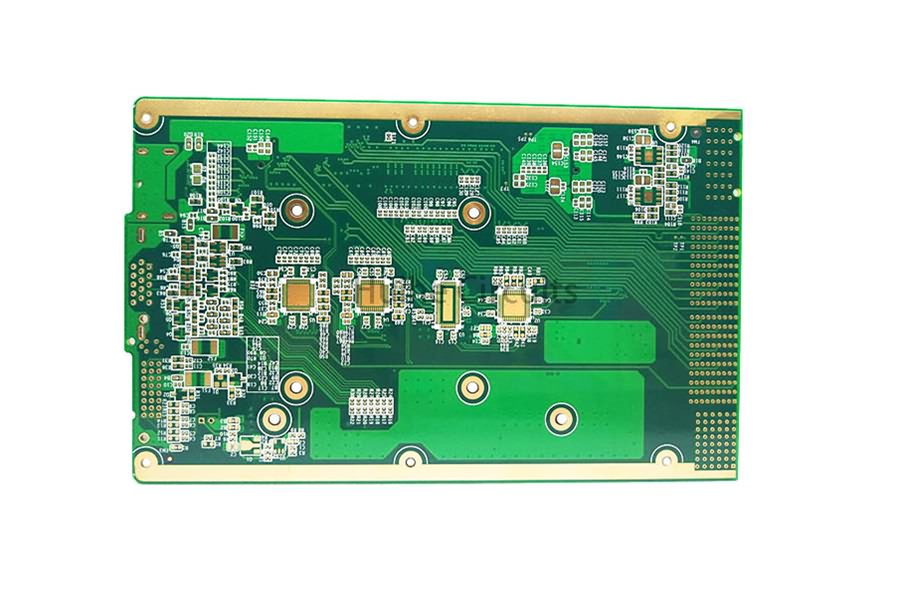
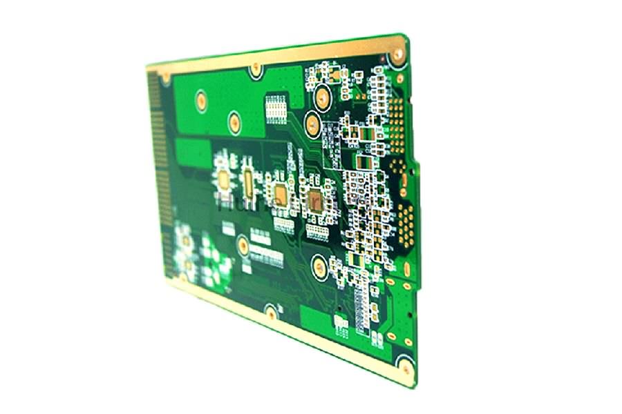
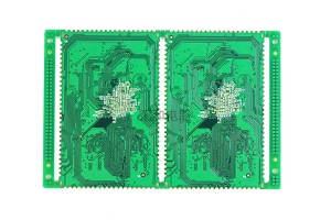
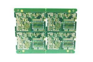
8 Layer ENIG Multilayer FR4 PCB

Multilayer PCB Design Advantages
1.Compared with single-sided PCB and double-sided PCB, it has higher density.
2.No interconnect cable is required. It is the best choice for low weight PCB.
3.Multilayer PCBs have smaller sizes and save space.
4.EMI is very simple and flexible.
5.Durable and powerful.
Application Of Multilayer PCB
Multilayer PCB design is the basic requirement of many electronic components:
Accelerator
Mobile Transmission
Optical Fiber
Scanning Technology
File Server And Data Storage
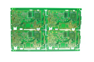
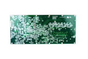
A Variety Of PCB Processes
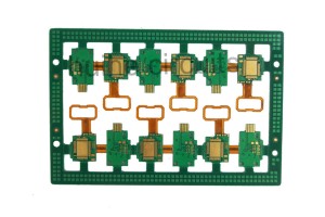
Rigid-Flex PCB
Flexible and thin, simplifying the product assembly process
Reduce connectors, high line carrying capacity
Used in image system and RF communication equipment
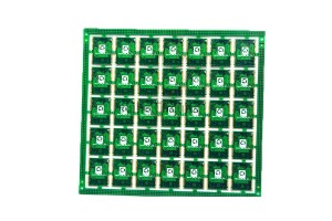
Half Hole PCB
There is no residual or warping of copper thorn in half hole
The child board of the mother board saves connectors and space
Applied to Bluetooth module, signal receiver
Impedance Control PCB
Strictly control the conductor width / thickness and medium thickness
Impedance linewidth tolerance ≤± 5%, good impedance matching
Applied to high-frequency and high-speed devices and 5g communication equipment
Blind Buried Via PCB
Use micro-blind holes to increase the line density
Improve radio frequency and electromagnetic interference, heat conduction
Apply to servers, mobile phones, and digital cameras