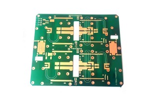
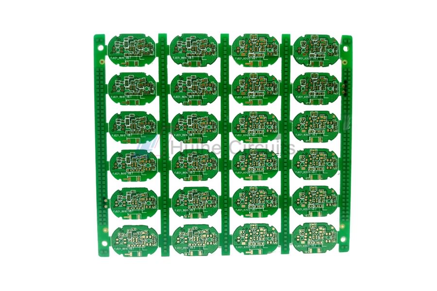
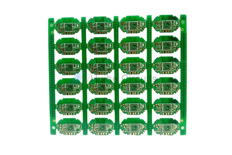
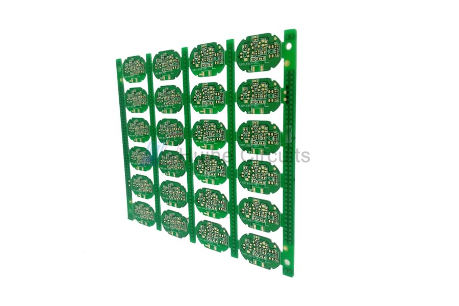
6 Layer ENIG Via-In-Pad PCB
Advantages Of The Plug Hole
1. The plug hole can prevent PCB through the wave soldering tin from the through hole through the component surface caused by short circuit; That is to say, within the scope of the wave soldering design area (generally the welding surface is 5mm or above) there is no hole or hole to do plug hole treatment.
2. The plug hole protects against possible short circuits caused by closely spaced devices such as BGA. This is the reason for the hole under the BGA to keep the hole in the design process. Because there is no plug hole, this is a case of short circuit.
3. Avoid flux residue in the conduction hole;
4. After the surface mounting and component assembly of the electronics factory is completed, the PCB shall be vacuum absorbed and negative pressure formed on the test machine before completion:
5. Prevent the surface solder paste into the hole caused by virtual welding, affect the installation; This point is most obvious in the heat dissipation pad with holes.
6. To prevent the wave soldering tin beads pop up, resulting in a short circuit.
7. The plug hole will be helpful to the SMT process.
Equipment Display

PCB Automatic Plating Line

PCB PTH Line

PCB LDI

PCB CCD Exposure Machine
Factory Show

PCB Manufacturing Base

Admin Receptionist

Meeting Room