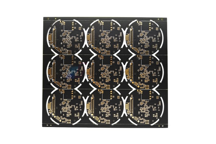
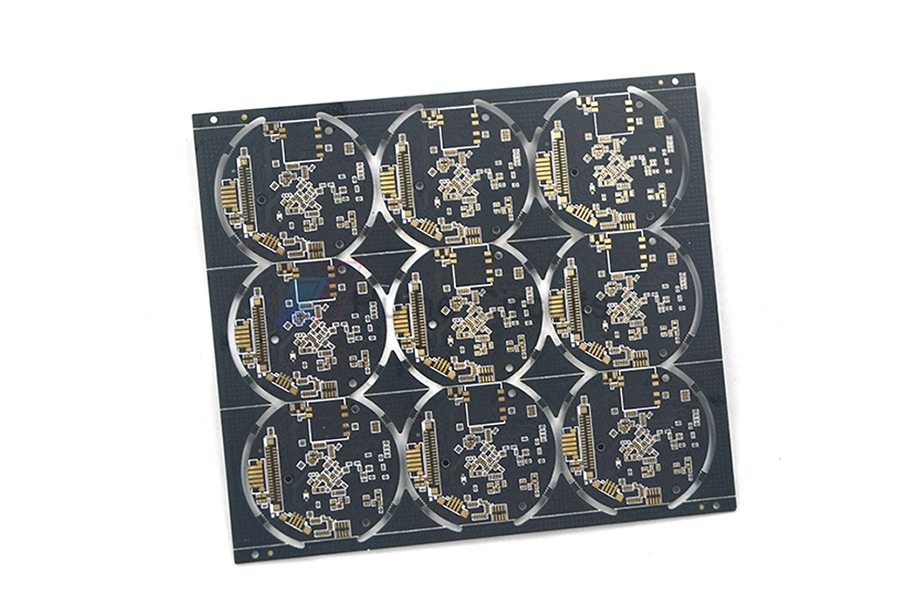
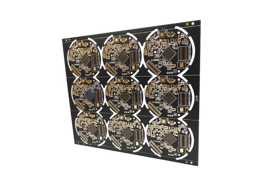
6 Layer ENIG FR4 Heavy Copper PCB
Crack problem of inner thick brazing pad
The demand for heavy copper PCB is increasing, and the inner layer pads are getting smaller and smaller. The problem of pad cracking often occurs during PCB drilling (mainly for large holes above 2.5mm).
There is little room for improvement in the material aspect of this kind of problem. The traditional improvement method is to increase the pad, increase the peeling strength of the material, and reduce the drilling rate, etc.
Based on the analysis of PCB processing design and technology, the improvement plan is put forward: copper cutting treatment (when etching the inner layer of the solder pad, the concentric circles smaller than the aperture are etched) is carried out to reduce the pulling force of copper during drilling.
Drilling a drill hole that is 1.0mm smaller than the required aperture, and then carry out normal aperture drilling (secondary drilling) to solve the crack problem of inner thickness brazing pad.
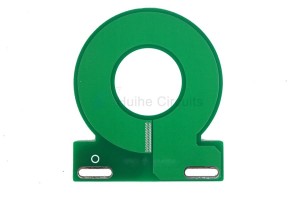
Applications of the heavy copper PCB
Heavy copper PCB is used for a variety of purposes, e.g. in flat transformers, heat transmission, high power dispersion, control converters, etc. In PC, automotive, military and mechanical control. A large number of copper PCBs are also used:
Power supply and control converter
Welding tools or equipment
The automobile industry
Solar panel manufacturers, etc
Equipment display

Automatic Plating Line

PTH line

LDI

CCD Exposure Machine
Our factory