2 Layer HASL High Tg Heavy Copper PCB
About The Heavy Copper PCB
Heavy copper PCB has the characteristics of carrying large current, reducing thermal strain and good heat dissipation. Increasing copper thickness has become an effective way for many terminal design manufacturers to seek solutions. There are more and more heavy copper PCB products, as a special product in product design, CCL production and PCB processing, there are many production difficulties and matters needing attention and solution.
(1)CCL is the raw material of PCB, and the structure design and process quality control of thick copper CCL are crucial to the reliability of subsequent heavy copper PCB products. In order to solve the problem of heavy copper PCB thin-core pressure resistance, CCL manufacturers have made very mature research on the selection of heavy copper PCB core copper foil and the design of the corresponding material. In order to solve the problem of thermal conductivity and adhesive filling of heavy copper PCB, some specially developed CCL and adhesive sheet for heavy copper PCB
(2)The design of the product including the manufacturability, craft workability and the reliability of the product engineering design PCB for subsequent processing has a very important role in the intuitively, in view of the thick copper products production difficulties we improve lining are put forward for design spread uniformity and symmetry, improve the inner residual copper rate, increasing the line width line spacing, and to optimize the design of the inner pad, etc
(3)There are many difficulties in PCB processing etching, laminating, drilling, welding resistance and other processes of heavy copper PCB. It is a kind of special plate with more difficulty in production. Pay attention to the details of each link in order to better produce heavy copper PCB with good quality.
With the continuous development of PCB technology, the design of various structures is becoming more and more strict, and the structural problems of thick copper multilayer PCBs are becoming more and more prominent. It is the continuous progress of these technologies that promotes the continuous improvement and improvement of materials.
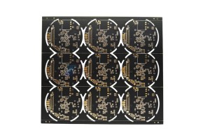
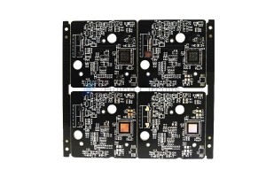
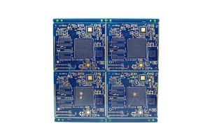
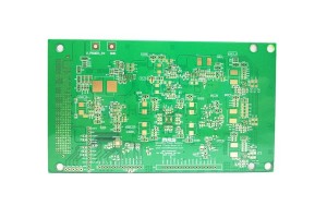
Equipment Display

PCB Automatic Plating Line

PCB PTH Line

PCB LDI